
Chen Wei, Wencong Wang, Dongmei Liu, Min Gu, Xianqiu Wu, "High-efficiency and large light-receiving area superconducting nanowire single-photon detector integrated with high-contrast grating," Photonics Res. 9, 2253 (2021)
- Photonics Research
- Vol. 9, Issue 11, 2253 (2021)
Abstract
1. INTRODUCTION
Since Gol’tsman’s first demonstration of the superconducting nanowire single-photon detector (SNSPD) [1] in 2001, it has undergone tremendous development [2–4]. Featuring high system detection efficiency [5–7], low dark count rate [8], short recovery time [9], and extremely low timing jitter [10], it has been used in a wide range of fields, such as quantum key distribution [11], laser ranging [12,13], space laser communication [14–16], and depth imaging [17]. However, compared with photomultiplier tubes or single-photon avalanche diodes (detection area from 100 μm to several millimeters in diameter), a typical single-pixel SNSPD detection area is usually only 10 μm in diameter [18], which limits the application of SNSPDs in certain scenarios, such as coupling with multi-mode fibers in deep space communications and lidar [19,20].
Increasing the effective detection area of the SNSPD is challenging. There are two main approaches to solving this problem. One of them is to increase the coverage area of the nanowires. Thus far, the maximum detection area of single-pixel SNSPDs with high efficiency is 100 μm in diameter, achieving a detection efficiency of 65% at 532 nm [21]. Another approach is to build SNSPD arrays to obtain a larger detection area by increasing the number of pixels. Few efficient large-area SNSPD arrays have been reported, such as a 16-pixel SNSPD with an effective area of
In this study, we adopt a novel approach of integrating optical structures in SNSPDs to increase the effective detection area of the detector without enlarging the area of the nanowires. A high-contrast grating (HCG) optical structure [25], which is a subwavelength grating structure inscribed with a high-refractive-index difference, is used. Owing to its large refractive index difference and subwavelength size, HCG can provide high reflectivity or high transmissivity over a large bandwidth. Moreover, it possesses an interesting property: the ability to control the phase shift of reflected/transmitted light [26]. If the structural parameters of a grating, such as the period, duty cycle, and thickness, are changed, the phase shift of the reflected/transmitted light changes accordingly. This implies that we can control the phase shift of the light to focus on the reflected/transmitted side while maintaining a high reflectance/transmittance [27,28]. Shiono
In this study, we theoretically propose a design method that integrates HCG with focusing capability into SNSPD (HCG-SNSPD). The simulation results show that the transverse magnetic (TM)-polarized incident light at a wavelength of 1550 nm passes through the
2. METHODS
A structural diagram of the HCG-SNSPD is shown in Fig. 1(a). HCG is located at the top of the structure. Si is selected as the grating material because of its high refractive index and its lack of absorption of incident light at 1550 nm. There is a vacuum gap between the gratings. Below the grating is a silicon dioxide (
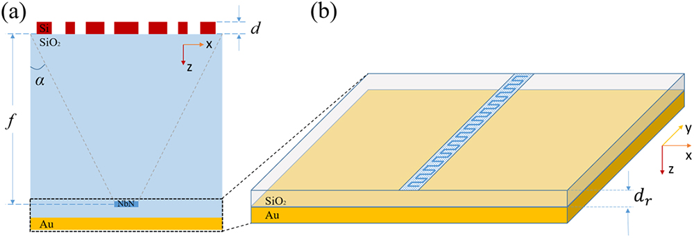
Figure 1.(a) Schematic diagram of the structure of HCG-SNSPD. HCG is located at the top of the structure. It is made of a high-refractive-index material Si with a thickness of
A detailed 3D schematic of the nanowires and resonant cavity below the structure is shown in Fig. 1(b). The shaded part above the
A schematic design of the HCG structure is shown in Fig. 2(a), which is divided into upper and lower parts. The upper part of Fig. 2(a) shows a 3D model of the HCG with TM-polarized light incident from the top, downwards along the
![]()
Figure 2.(a) Schematic diagram of HCG design. The upper part is a 3D structural view of the grating. The TM-polarization plane wave is incident from the top, downwards toward the HCG. The lower part is the front view of the grating along the
To design a focused HCG, it is necessary to obtain the ideal phase shift distribution [the black curve in Fig. 2(b) of the transmitted light according to Eq. (1)]. Thereafter, we select the grating parameters that satisfy this phase shift distribution according to each spatial position. To achieve effective focus while ensuring a high transmittance, each grating bar is required to have high transmittance (
Considering processing difficulty, the thickness of the gratings is chosen as 0.75 μm. According to our calculations, a thickness greater than or less than 0.75 μm will cause the phase shift table controlled by parameters
Figures 2(c) and 2(d) show the data tables of transmittance and phase shift corresponding to each
To investigate the relationship between the focal length and transmittance of the corresponding focal plane [blue square line in Fig. 2(b)], we designed a few sets of HCGs with the same number of grating bars (
The red discrete dots in Fig. 2(b) are the phase shifts corresponding to each grating bar in our design for HCG with
Figure 3(a) shows the cross-sectional normalized energy distribution; the HCG is at the top position at
![]()
Figure 3.Simulation results of the designed HCG with
Additionally, the HCG also has a high transmittance of incident light. Figure 4(a) shows the transmittance spectra of the entire focal plane (
![]()
Figure 4.(a) Transmittance spectrum at the focal plane. The red, blue, and green solid lines indicate the transmittance across the focal plane, the central 30-μm width, and the central 10-μm width, respectively. (b) Absorption of nanowire as a function of
So far, we have verified the satisfactory focusing property and transmission effect of HCG that promises a possibility of the efficient absorption of incident light from a large area to a small area of nanowires. However, a new problem is encountered here: HCG causes a deflection of the vertical incident light. If the nanowires are placed at the focal point, the angle between the incident light and the nanowires is no longer 90°. To investigate the effect of this factor on absorption, we attempted to illuminate the nanowires with plane waves at different incident angles and obtain the absorption versus incident angle [Fig. 4(b)]. The inset shows the simulated structure. The source was placed in the
3. RESULTS AND ANALYSIS
We integrated the HCG with the SNSPD as shown in Fig. 1(a) and placed the nanowires at the focal point. The absorption efficiency of the detector (without the Au mirror) as a function of wavelength is indicated with blue dots in Fig. 5(a). In the range of 1480–1640 nm, the detector achieves an absorption efficiency of more than 30% with a peak absorption of 33.53% at 1540 nm. It is an appropriate absorption efficiency without auxiliary structures, but it is still not sufficient for practical applications. Therefore, we insert an optical resonant cavity structure of metal–insulator nanowires underneath the nanowires to improve the absorption efficiency of the detector. The structure of the resonant cavity is described in the description of Fig. 1(b). We explored the relationship between the cavity thickness
![]()
Figure 5.(a) Absorption spectrum of HCG-SNSPD. The red squares and blue dots indicate the absorption with and without cavity structure, respectively. The inset shows the normalized energy field distribution results for the nanowire integrated with the cavity at the wavelength of 1550 nm. The widths of the field area in the horizontal and vertical directions are 18 μm and 4 μm, respectively. The nanowires are located in the dotted rectangle. (b) Absorption efficiency as a function of resonant cavity thickness (
After obtaining the optical cavity thickness
In addition, we investigated the influence of the filling factor of the nanowires on the absorption. The thickness of the resonant cavity was considered as
![]()
Figure 6.Absorption efficiency as a function of the filling factor. The red squares and blue triangles indicate the absorption of nanowires with 8-nm and 6-nm thickness, with different filling factors, respectively. The inset shows a schematic diagram of the filling factor.
We have theoretically verified the effectiveness of HCG-SNSPD with an example of
Figure 7(a) shows the influence on absorption when the thickness and width of the grating are varied. The thickness
![]()
Figure 7.Influence of fabrication tolerances on absorption results (at the wavelength of 1550 nm). (a) Absorption as a function of the thickness
Besides the grating, the position of the nanowires may be deviated because of the overlay accuracy, which means that they may not be perfectly placed at the center of the focus. We have fully considered this tolerance in the preparation process at the beginning of the design of the structure. The possible horizontal and vertical deviations of the nanowire positions are illustrated in the inset of Fig. 7(b). The deviation here refers to the distance that the center point of the nanowires moves in the horizontal or vertical direction. For the horizontal deviation [blue line in Fig. 7(b)], there is a very small decrease in absorption in the range of 3.5 μm, but the overall remains above 80%. When the deviation is greater than 3.5 μm, the decreasing slope of the absorption starts to increase rapidly. This phenomenon is easy to explain. The width of the focal spot is
4. DISCUSSION
We have proved that SNSPD integrated with HCG can achieve high-efficiency broadband detection in the NIR band with a large light-receiving area. Prior to our work, phase gratings and metal–insulator–metal (MIM) circular gratings were integrated into SNSPD to increase its light-receiving area [33,34].
In addition to the method of using integrated gratings to achieve large receiving areas for SNSPDs, lenses are also used in SNSPDs to achieve convergence of light. Zhang
In the latest study, Xu
5. CONCLUSION
In summary, we theoretically propose a large light-receiving area and high-efficiency SNSPD integrated with HCG. Utilizing the characteristics of high transmittance and phase shift control of HCG, we designed the HCG with a focal length
References
[1] G. N. Gol’tsman, O. Okunev, G. Chulkova, A. Lipatov, A. Semenov, K. Smirnov, B. Voronov, A. Dzardanov, C. Williams, R. Sobolewski. Picosecond superconducting single-photon optical detector. Appl. Phys. Lett., 79, 705-707(2001).
[2] C. M. Natarajan, M. G. Tanner, R. H. Hadfield. Superconducting nanowire single-photon detectors: physics and applications. Supercond. Sci. Technol., 25, 063001(2012).
[3] I. Holzman, Y. Ivry. Superconducting nanowires for single-photon detection: progress, challenges, and opportunities. Adv. Quantum Technol., 2, 1800058(2019).
[4] D. Li, R. Jiao. Design of a low-filling-factor and polarization-sensitive superconducting nanowire single photon detector with high detection efficiency. Photon. Res., 7, 847-852(2019).
[5] P. Hu, Y. Ma, H. Li, Z. Liu, H. Yu, J. Quan, Y. Xiao, L. You, Y. Liu, J. Liang, Z. Wang. Superconducting single-photon detector with a system efficiency of 93% operated in a 2.4 K space-application-compatible cryocooler. Supercond. Sci. Technol., 34, 07LT01(2021).
[6] D. V. Reddy, R. R. Nerem, S. W. Nam, R. P. Mirin, V. B. Verma. Superconducting nanowire single-photon detectors with 98% system detection efficiency at 1550 nm. Optica, 7, 1649-1653(2020).
[7] H. Li, Y. Wang, L. You, H. Wang, H. Zhou, P. Hu, W. Zhang, X. Liu, X. Yang, L. Zhang, Z. Wang, X. Xie. Supercontinuum single-photon detector using multilayer superconducting nanowires. Photon. Res., 7, 1425-1431(2019).
[8] H. Shibata, K. Shimizu, H. Takesue, Y. Tokura. Ultimate low system dark-count rate for superconducting nanowire single-photon detector. Opt. Lett., 40, 3428-3431(2015).
[9] A. Vetter, S. Ferrari, P. Rath, R. Alaee, O. Kahl, V. Kovalyuk, S. Diewald, G. N. Goltsman, A. Korneev, C. Rockstuhl, W. H. P. Pernice. Cavity-enhanced and ultrafast superconducting single-photon detectors. Nano Lett., 16, 7085-7092(2016).
[10] B. Korzh, Q. Zhao, J. P. Allmaras, S. Frasca, T. M. Autry, E. A. Bersin, A. D. Beyer, R. M. Briggs, B. Bumble, M. Colangelo, G. M. Crouch, A. E. Dane, T. Gerrits, A. E. Lita, F. Marsili, G. Moody, C. Peña, E. Ramirez, J. D. Rezac, N. Sinclair, M. J. Stevens, A. E. Velasco, V. B. Verma, E. E. Wollman, S. Xie, D. Zhu, P. D. Hale, M. Spiropulu, K. L. Silverman, R. P. Mirin, S. W. Nam, A. G. Kozorezov, M. D. Shaw, K. K. Berggren. Demonstration of sub-3 ps temporal resolution with a superconducting nanowire single-photon detector. Nat. Photonics, 14, 250-255(2020).
[11] K. Takemoto, Y. Nambu, T. Miyazawa, Y. Sakuma, T. Yamamoto, S. Yorozu, Y. Arakawa. Quantum key distribution over 120 km using ultrahigh purity single-photon source and superconducting single-photon detectors. Sci. Rep., 5, 14383(2015).
[12] H. Li, L. Zhang, L. You, X. Yang, W. Zhang, X. Liu, S. Chen, Z. Wang, X. Xie. Large-sensitive-area superconducting nanowire single-photon detector at 850 nm with high detection efficiency. Opt. Express, 23, 17301-17308(2015).
[13] L. Xue, M. Li, L. Zhang, D. Zhai, Z. Li, L. Kang, Y. Li, H. Fu, M. Ming, S. Zhang, X. Tao, Y. Xiong, P. Wu. Long-range laser ranging using superconducting nanowire single-photon detectors. Chin. Opt. Lett., 14, 071201(2016).
[14] M. E. Grein, A. J. Kerman, E. A. Dauler, O. Shatrovoy, R. J. Molnar, D. Rosenberg, J. Yoon, C. E. DeVoe, D. V. Murphy, B. S. Robinson, D. M. Boroson. Design of a ground-based optical receiver for the lunar laser communications demonstration. International Conference on Space Optical Systems and Applications (ICSOS), 78-82(2011).
[15] H. Ivanov, E. Leitgeb, P. Pezzei, G. Freiberger. Experimental characterization of SNSPD receiver technology for deep space FSO under laboratory testbed conditions. Optik, 195, 163101(2019).
[16] X. Li, J. Tan, K. Zheng, L. Zhang, L. Zhang, W. He, P. Huang, H. Li, B. Zhang, Q. Chen, R. Ge, S. Guo, T. Huang, X. Jia, Q. Zhao, X. Tu, L. Kang, J. Chen, P. Wu. Enhanced photon communication through Bayesian estimation with an SNSPD array. Photon. Res., 8, 637-641(2020).
[17] S. Chen, D. Liu, W. Zhang, L. You, Y. He, W. Zhang, X. Yang, G. Wu, M. Ren, H. Zeng, Z. Wang, X. Xie, M. Jiang. Time-of-flight laser ranging and imaging at 1550 nm using low-jitter superconducting nanowire single-photon detection system. Appl. Opt., 52, 3241-3245(2013).
[18] S. Steinhauer, S. Gyger, V. Zwiller. Progress on large-scale superconducting nanowire single-photon detectors. Appl. Phys. Lett., 118, 100501(2021).
[19] H. Hemmati, A. Biswas, I. B. Djordjevic. Deep-space optical communications: future perspectives and applications. Proc. IEEE, 99, 2020-2039(2011).
[20] C. Yu, J. Qiu, H. Xia, X. Dou, J. Zhang, J. Pan. Compact and lightweight 1.5 μm lidar with a multi-mode fiber coupling free-running InGaAs/InP single-photon detector. Rev. Sci. Instrum., 89, 103106(2018).
[21] C. L. Lv, H. Zhou, H. Li, L. X. You, X. Y. Liu, Y. Wang, W. J. Zhang, S. J. Chen, Z. Wang, X. M. Xie. Large active area superconducting single-nanowire photon detector with a 100 μm diameter. Supercond. Sci. Technol., 30, 115018(2017).
[22] Q. Chen, B. Zhang, L. Zhang, R. Ge, R. Xu, Y. Wu, X. Tu, X. Jia, D. Pan, L. Kang, J. Chen, P. Wu. Sixteen-pixel NbN nanowire single photon detector coupled with 300-μm fiber. IEEE Photon. J., 12, 6800112(2020).
[23] J. P. Allmaras, A. D. Beyer, R. M. Briggs, F. Marsili, M. D. Shaw, G. V. Resta, J. A. Stern, V. B. Verma, R. P. Mirin, S. W. Nam, W. H. Farr. Large-area 64-pixel array of WSi superconducting nanowire single photon detectors. Conference on Lasers and Electro-Optics (CLEO), 1-2(2017).
[24] M. Yabuno, S. Miyajima, S. Miki, H. Terai. Scalable implementation of a superconducting nanowire single-photon detector array with a superconducting digital signal processor. Opt. Express, 28, 12047-12057(2020).
[25] C. J. Chang-Hasnain, W. Yang. High-contrast gratings for integrated optoelectronics. Adv. Opt. Photon., 4, 379-440(2012).
[26] D. Fattal, J. Li, Z. Peng, M. Fiorentino, R. G. Beausoleil. Flat dielectric grating reflectors with focusing abilities. Nat. Photonics, 4, 466-470(2010).
[27] F. Lu, F. G. Sedgwick, V. Karagodsky, C. Chase, C. J. Chang-Hasnain. Planar high-numerical-aperture low-loss focusing reflectors and lenses using subwavelength high contrast gratings. Opt. Express, 18, 12606-12614(2010).
[28] W. Fang, Y. Huang, J. Fei, X. Duan, K. Liu, X. Ren. Concentric circular focusing reflector realized using high index contrast gratings. Opt. Commun., 402, 572-576(2017).
[29] T. Shiono, M. Kitagawa, K. Setsune, T. Mitsuyu. Reflection micro-Fresnel lenses and their use in an integrated focus sensor. Appl. Opt., 28, 3434-3442(1989).
[30] L. Redaelli, G. Bulgarini, S. Dobrovolskiy, S. N. Dorenbos, V. Zwiller, E. Monroy, J. M. Gérard. Design of broadband high-efficiency superconducting-nanowire single photon detectors. Supercond. Sci. Technol., 29, 065016(2016).
[31] C. Ma, Y. Huang, X. Ren. High-numerical-aperture high-reflectivity focusing reflectors using concentric circular high-contrast gratings. Appl. Opt., 54, 973-978(2015).
[32] L. Zhang, C. Wan, M. Gu, R. Xu, S. Zhang, L. Kang, J. Chen, P. Wu. Dual-lens beam compression for optical coupling in superconducting nanowire single-photon detectors. Sci. Bull., 60, 1434-1438(2015).
[33] M. Gu, L. Kang, L. Zhang, Q. Zhao, T. Jia, C. Wan, R. Xu, X. Yang, P. Wu. A high-efficiency broadband superconducting nanowire single-photon detector with a composite optical structure. Chin. Phys. Lett., 32, 038501(2015).
[34] S. Wang, F. Chen, Y. Zhang, Q. Li, X. Sun, X. Chen, W. Lu. Simulation of superconducting single photon detector coupled with metal-insulator-metal circular grating. 13th International Conference on Numerical Simulation of Optoelectronic Devices (NUSOD), 131-132(2013).
[35] S. Miki, T. Yamashita, M. Fujiwara, M. Sasaki, Z. Wang. Multichannel SNSPD system with high detection efficiency at telecommunication wavelength. Opt. Lett., 35, 2133-2135(2010).
[36] L. You, J. Quan, Y. Wang, Y. Ma, X. Yang, Y. Liu, H. Li, J. Li, J. Wang, J. Liang, Z. Wang, X. Xie. Superconducting nanowire single photon detection system for space applications. Opt. Express, 26, 2965-2971(2018).
[37] J. Yu, R. Zhang, Y. Gao, Z. Sheng, M. Gu, Q. Sun, J. Liao, T. Wu, Z. Lin, P. Wu, L. Kang, H. Li, L. Zhang, W. Zheng. Intravital confocal fluorescence lifetime imaging microscopy in the second near-infrared window. Opt. Lett., 45, 3305-3308(2020).
[38] Y. Xu, A. Kuzmin, E. Knehr, M. Blaicher, K. Ilin, P.-I. Dietrich, W. Freude, M. Siegel, C. Koos. Superconducting nanowire single-photon detector with 3D-printed free-form microlenses. Opt. Express, 29, 27708-27731(2021).


Set citation alerts for the article
Please enter your email address

© Copyright 2018-2021 | Chinese Laser Press. All Rights Reserved 沪ICP备15018463号-20