
Bingbing Chen, Pengyang Wang, Ningyu Ren, Renjie Li, Ying Zhao, Xiaodan Zhang. Tin dioxide buffer layer-assisted efficiency and stability of wide-bandgap inverted perovskite solar cells[J]. Journal of Semiconductors, 2022, 43(5): 052201
- Journal of Semiconductors
- Vol. 43, Issue 5, 052201 (2022)
Abstract
1. Introduction
Recently, a record power conversion efficiency (PCE) of perovskite/silicon monolithic tandem solar cells has increased to 29.8%[
Up to now, the PCE of IPSCs has reached to 23.37% with a certificate efficiency of 22.75%[
Besides the PCE, the main challenge for actual commercialization in PSCs lies instability[
Here, SnO2 using the atomic layer deposition (ALD) method was designed as an additional buffer layer on the BCP layer for improving efficiency and stability in wide bandgap IPSCs. Compared with previous methods, ultra-thin and compact SnO2 could be obtained by ALD process. Moreover, vacuum conditions and suitable for large area fabrication also make it great potential for future commercialization. It was found that SnO2 layer was homogeneously coated on the sample surface eliminating the possible leakage current and thus raising the shunt resistance (Rsh) and reducing the reverse current (J0). Finally, 21.13% efficiency was obtained in the wide-bandgap (1.63 eV) inverted perovskite device with a SnO2 additional buffer layer. Moreover, ALD growing SnO2 layer with a great compactness which enhanced the moisture contact angle and improved stability of the perovskite device.
2. Experimental section
2.1. Device fabrication
ITO substrates were cleaned by detergent, DI water, acetone and isopropanol for 30 min, respectively. Then the substrates were treated by UV-ozone for 20 min. And then, PTAA (5 mg/mL in CB) solution was spin-coated onto the substrates at 5000 rpm for 30 s and annealed at 100 °C for 10 min in the glovebox with nitrogen condition. 1.5 M PbI2 : PbBr2 (83 : 17) precursor solution was spin-coated onto PTAA at the speed of 3000 rpm for 30 s and annealed at 70 °C for 1 min. And then, a mixture solution of organic salt (FAI : MABr : MACl = 90 : 6 : 9) was spin-coated onto the film at a speed of 3500 rpm for 30 s followed by annealing at 150 °C for 20 min in ambient air (30%–40% humidity). The passivation layer GABr (3 mg/mL in IPA) was fabricated by spin-coating at 5000 rpm for 30 s followed by annealing at 100 °C for 5 min. Subsequently, PCBM solution (20 mg/mL in CB) was spin-coated onto the perovskite film at a speed of 1500 rpm for 30 s. BCP solution (0.5 mg/mL in IPA) was spin-coated onto the PCBM film at a speed of 5000 rpm for 30 s. And then, the devices were moved into ALD devices to deposit SnO2 film with different thicknesses. The deposition of the SnO2 with the following processing sequence: 0.5 s TDMASn pulse, 15 s purge (20 sccm N2), 0.1 s deionized water pulse, and 15 s purge (20 sccm N2) at 85 °C. Finally, 150 nm of Cu top electrode were thermally evaporated under vacuum with a shadow mask. The area of the cells is 0.12 cm2, when measuring, a 0.0887 cm2 mask was used to define the accurate aperture area for the cells.
2.2. Material and device characterizations
2.2.1. Materials
Lead bromide (PbBr2), chlorobenzene (CB), dimethylsulfoxide (DMSO), N, N-dimethylformamide (DMF) and isopropyl alcohol (IPA) were purchased from Sigma-Aldrich. Polybis (4-phenyl) (2,4, 6-trimethyl-phenyl) amine (PTAA), [6,6]-Phenyl C61 butyric acid methyl ester (PCBM), bathocuproine (BCP), lead iodide (PbI2), bromide guanidine (GABr), formamidinium iodide (FAI), methylammonium bromide (MABr), and methylammonium chloride (MACl) were purchased from Xi’an Polymer Light Technology Corp.
2.2.2. Device characterizations
Scanning electron microscopy (SEM, FEI NanoSEM650) was used to characterize the morphology of the SnO2 films and also the cross-sectional image of the fully device. The current density–voltage (J–V) characteristics of the devices were measured by Keithley 2400 Source meter under AM 1.5G illumination with Xenon-lamp based solar simulator (Enli. Tec., Taiwan). The intensity of the light was calibrated with KG-5 filter Si photodiode. And the area of the solar cells was 0.08875 cm2. When measuring the device performance, a metal mask was used to reduce the influence of the scattered light. The forward scan (0–1.2 V, scan rate 20 mV/s, delay time 20 ms) and reverse scan (1.2–0 V, scan rate 20 mV/s, delay time 20 ms) were applied. External quantum efficiency (EQE) spectra were conducted by Enli Tec (Taiwan) measurement system in the wavelength from 300 to 900 nm with a scanning step of 10 nm. The photoluminescence (PL) and time-resolved photoluminescence (TRPL) spectroscopies were measured with a laser wavelength of 475 nm and power of 0.2 mW (Edinburgh FS5). The root mean square (RMS) roughness of different films was taken from atomic force microscopy (AFM) images measured with ARTCAM-130-SIINT (ARTRAY Co. Ltd., Japan).
3. Results and discussion
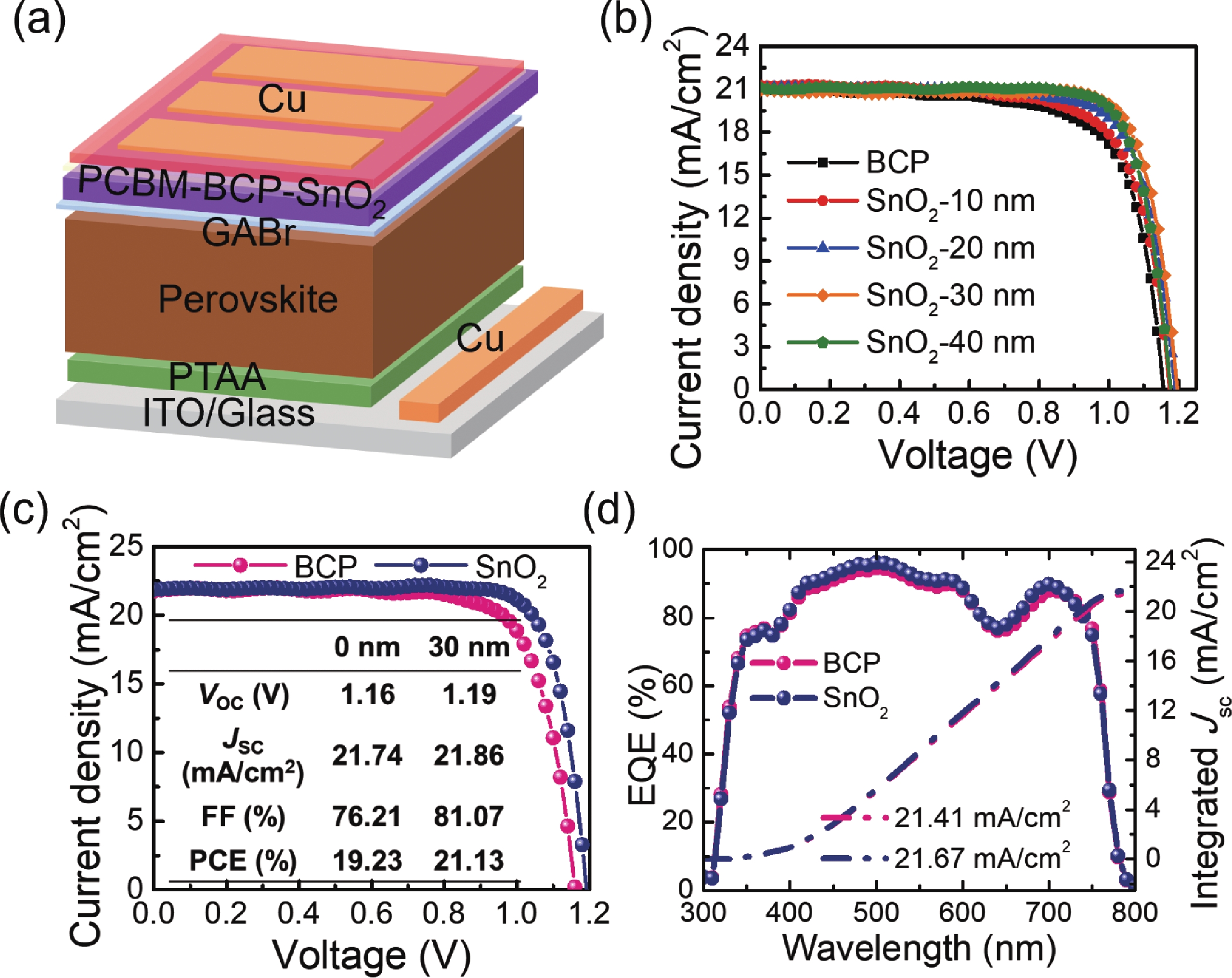
Firstly, SnO2 with different thickness as an additional buffer layer is designed. Fig. 1(a) presents the illustration of the IPSCs devices with a structure of ITO/PTAA/Perovskite/PCBM/BCP/SnO2/Cu. The thickness of perovskite film is around 550 nm (Fig. S1). Current density–voltage (J–V) curves of the devices with SnO2 films of different thicknesses (0, 10, 20, 30, 40 nm) are shown in Fig. 1(b). The results demonstrate that the devices with SnO2 layer obtain a higher VOC and fill factor (FF), short-circuit current density (JSC) is also slightly increased. The control device without SnO2 layer achieves a PCE of 17.47%. When the thickness of SnO2 film increased from 10–30 nm, the PCE is enhanced to 17.60, 18.29 and 20.02, respectively. While the thickness of SnO2 increased to 40 nm, the performance of IPSCs decreased to 19.82%, which may be due to the thick SnO2 film introducing a high series resistance. The performance of IPSCs with different scanning directions are presented in Fig. S2 and Table S1. And the statistical diagrams of the device performances are shown in Fig. S3. After optimization, the device of 30 nm SnO2 exhibited champion performance with a VOC of 1.19 V, JSC of 21.86 mA/cm2, FF of 81.07%, and the corresponding PCE of 21.13%. While, the control device only with a PCE of 19.23%.
![]()
Figure 1.(Color online) Device structure and performance with different SnO2 thickness. (a) The architecture of the device in this work. (b)
J–V and external quantum efficiency (EQE) curves are presented in Figs. 1(c) and 1(d), respectively. The integral current densities of the devices are 21.41 and 21.67 mA/cm2 which are well matched with the JSC in J–V measurement. The bandgap of the perovskite can be determined by the tangent of the curve to the base line which is also presented. The ultraviolet-visible absorption of perovskite material and (αhν)2 versus energy of perovskite film are shown in Fig. S4. It can be found that the bandgap of the perovskite is about 1.63 eV. Therefore, the VOC deficit (Eg/q–VOC) is only of 440 mV. This value is a lower VOC loss which compares to other wide bandgap IPSCs as present in Table S2. Moreover, device performance of different SnO2 thicknesses with or without BCP are also investigated (Fig. S5). BCP is essential when a thinner SnO2 is deposited. With increasing the thickness of SnO2, the role of BCP is gradually diminished. Devices with BCP and a suitable thicker SnO2 buffer layer achieved a higher FF and PCE.
Time-resolved photoluminescence (TRPL) is employed to investigate the transport and recombination dynamics of photoinduced carriers in perovskite films without and with 30 nm SnO2 buffer layer (Fig. 2(a)). The biexponential function is applied to fit the TRPL decay curves (Eq. (1))[
![]()
Figure 2.(Color online) Device performance without the SnO2 buffer layer and with 30 nm SnO2 buffer layer. (a) TRPL curves of the devices. (b)
where τ1 and τ2 are the lifetimes for the carrier transport and recombination, and A1 and A2 are the corresponding amplitudes. τ1 is due to the carrier transport occurring in the surface of the perovskite film, whereas τ2 could be attributed to the bulk and surface recombination. The devices without SnO2 obtained τ1 = 42.01 ns and τ2 = 146.43 ns, respectively. While τ1 = 37.65 ns and τ2 = 181.59 ns are given with SnO2. The decrease of τ1 indicates faster electron transfer from perovskite to ETL with the presence of SnO2. The increased τ2 indicates a slower recombination rate. The film with defferent thickness of SnO2 film were also presented in Fig. S6, and the fitting value of the carrier transport and recombination lifetime were shown in Table S3. The results illustrate that perovskite film with SnO2 additional layer achieves a faster carrier extraction and a lower carrier quenching between the active layer and the transport layer, which is a good agreement with the higher FF and VOC.Rsh of the devices without or with 30 nm SnO2 are also calculated (Fig. 2(b)). The higher Rsh benefits the enhancement of the FF, which further confirms the excellent function of the SnO2 buffer layer.
Fig. 2(c) shows the dark J–V curves of the devices without and with a 30 nm SnO2 buffer layer. According to the Schottky junction model, diode ideality factor (n) and J0 can be obtained by fitting the linear J–V curve (exponential diode behavior region) as shown in Fig. 2(d). The Eq. (2) shows in the following[
where J is the current density value, V is the applied voltage, T is the absolute temperature, k is the Boltzmann constant, e is the electron charge. From the equation we can find that n andJ0 are close related with the slope and intercept of the linear fitting of ln(J0) versus V. The control device has a slope of 16.41, while the device with 30 nm SnO2 film has a slope of 19.38. The larger the slope, the smaller the n, which proved a better diode characteristic. The corresponding J0 values of 1.10 × 10⁻⁹ and 1.22 × 10⁻⁸ mA/cm2 are obtained of the devices with and without SnO2 film. The results clearly indicated that device with SnO2 film has a lower J0, which means a smaller leakage current, resulting in a higher VOC.
A top-view scanning electron microscope (SEM) is primordially verified to show the surface morphology of the devices with or without SnO2 (Fig. 3). Figs. 3(a)–3(e) were the SnO2 film morphologies with the thickness of 0, 10, 20, 30 and 40 nm on the structure of glass/ITO/PTAA/perovskite/PCBM/BCP, respectively. As expected, SnO2 films with different thicknessness demonstrate different coverage, and the surface becomes increasingly compact as the thickness increases. SnO2 with 10 nm obtains the poorest coverage while all of the devices with thickness over 20 nm show uniform and dense morphology, and the device with 30 nm SnO2 has the best coverage. Fig. 3(f) shows a clearer morphology of SnO2 with the thickness of 30 nm, and it further illustrates that the compact SnO2 layer can uniform coverage of the ETL layer, obstructing the immediate contact with the metal electrode. And the illustrations present the corresponding surface morphology of the films with different thicknesses of SnO2 by an atomic force microscope (AFM). The root-mean-square (RMS) roughness of the films is shown in Fig. 3(g), SnO2 film deposited by ALD can effectively reduce surface roughness. The assumed schematic diagrams of the performance improvement are demonstrated in Figs. 3(h) and 3(i). Perovskites with a rough surface, so the solution method BCP with a thinner thickness may not cover the PCBM completely. This supplies an opportunity of direct contact between PCBM and metal electrode, causing a non-radiative recombination center and reducing the Rsh, and thus degrading the performance of the devices. Whereas, the ALD method SnO2 can conformal growth on the uneven surface which completely prevents the current leakage. That more distinctly illustrates the reason of the increased VOC and FF of the devices with SnO2 additional buffer layers.
![]()
Figure 3.(Color online) Top view SEM of SnO2 layer with various thicknesses based on the structure of ITO/PTAA/Perovskite/PCBM. (a), (b), (c), (d) and (e) with thickness of SnO2 of 0, 10, 20, 30 and 40 nm, respectively. (f) With a larger magnification to show a clearer morphology of SnO2 with the thickness of 30 nm. (g) RMS of the films with different thicknesses of SnO2. (h) The schematic diagram of the sample with a thinner BCP layer. (i) The schematic diagram of the sample with a BCP and SnO2 bilayer.
The water contact angles are presented in Figs. 4(a) and 4(b). It is evidently shown that the film with a 30 nm SnO2 layer has a larger contact angle which can better resistance to moisture and then stabilize the device. The devices without and with 30 nm SnO2 are stored in a glove box with nitrogen (N2) condition (Fig. S7). Both of the devices show relatively high stability, the device performance with SnO2 is basically keeping the same efficiency without decay after 600 h. Figs. 4(c)–4(e) show the normalized VOC, JSC and FF of the device with and without SnO2 layer in the air atmosphere with relative humidity between 20%–40% without encapsulation, respectively. Fig. 4(f) presents the normalized PCE of the devices with or without SnO2 layer. It is clearly shown that the device with SnO2 still maintains 90% of initial efficiency after 600 h. Nevertheless, the efficiency of the device without SnO2 drops down to less than its 70%. We can find that the attenuation of the PCE is mainly due to the decrease of FF and VOC, while the JSC are barely changed. Fig. S8 presents the changes of series resistance (Rs) for the two devices, we supposed the increased Rs is the reason for the FF and VOC losses.
![]()
Figure 4.(Color online) (a, b) The water contact angle of the device without and with SnO2. (c–f) Normalized
4. Conclusions
In summary, we have demonstrated that the ALD-processed SnO2 as an additional buffer layer in IPSCs is a general approach to enhance the device’s performance and stability. The results show that this additional buffer layer can significantly increase the Rsh and reduce the leakage current, thus enhancing the FF and VOC. Meanwhile, the uniform SnO2 film with good hydrophobicity to repelling moisture, which can retard the decomposition of perovskite film. The device with a SnO2 buffer layer achieves over 90% of its initial efficiency after 600 h under an ambient condition with relative humidity of 20%–40%. Instead, the control device only exhibits 70% of its initial efficiency. This work provides a facile way of boosting the efficiency and stability of IPSCs, which also gives guidance for perovskite-based tandem solar cells for future commercialization.
Acknowledgements
B.B. Chen and P.Y. Wang contributed equally to this work. The authors gratefully acknowledge the supports from National Key Research and Development Program of China (Grant No. 2018YFB1500103), the Overseas Expertise Introduction Project for Discipline Innovation of Higher Education of China (Grant No. B16027), Tianjin Science and Technology Project (Grant No. 18ZXJMTG00220), and the Fundamental Research Funds for the Central Universities, Nankai University (Grant Nos. 63191736, ZB19500204). Natural Science Foundation of Tianjin (No. 20JCQNJC02070). China Postdoctoral Science Foundation (No. 2020T130317).
Appendix A. Supplementary materials
Supplementary materials to this article can be found online at https://doi.org/10.1088/1674-4926/43/5/052201.
References
[1]
[2] B Chen, N Ren, Y Li et al. Insights into the development of monolithic perovskite/silicon tandem solar cells. Adv Energy Mater, 2003628(2021).
[3] F Hou, Y Li, L Yan et al. Control perovskite crystals vertical growth for obtaining high-performance monolithic perovskite/silicon heterojunction tandem solar cells with
[4] B Chen, P Wang, R Li et al. Composite electron transport layer for efficient n-i-p type monolithic perovskite/silicon tandem solar cells with high open-circuit voltage. J Energy Chem, 63, 461(2021).
[5]
[6] D Kim, H J Jung, I J Park et al. Efficient, stable silicon tandem cells enabled by anion-engineered wide-bandgap perovskites. Science, 368, 155(2020).
[7] J Xu, C C Boyd, Z J Yu et al. Triple-halide wide–band gap perovskites with suppressed phase segregation for efficient tandems. Science, 367, 1097(2020).
[8] C Zuo, L Ding. Drop-casting to make efficient perovskite solar cells under high humidity. Angew Chem Int Ed, 133, 11342(2021).
[9] F Li, X Deng, F Qi et al. Regulating surface termination for efficient inverted perovskite solar cells with greater than 23% efficiency. J Am Chem Soc, 142, 20134(2020).
[10] EL Unger, L Kegelmann, K Suchan et al. Correction: Roadmap and roadblocks for the band gap tunability of metal halide perovskites. J Mater Chem A, 5, 15983(2017).
[11] G Niu, W Li, J Li et al. Progress of interface engineering in perovskite solar cells. Sci China Mater, 59, 728(2016).
[12] C Xu, Z Zhang, Y Hu et al. Printed hole-conductor-free mesoscopic perovskite solar cells with excellent long-term stability using peai as an additive. J Energy Chem, 27, 764(2018).
[13] H Lu, Y Liu, P Ahlawat et al. Vapor-assisted deposition of highly efficient, stable black-phase FAPbI3 perovskite solar cells. Science, 370, eabb8985(2020).
[14] H Min, M Kim, S U Lee et al. Efficient, stable solar cells by using inherent bandgap of α-phase formamidinium lead iodide. Science, 366, 749(2019).
[15] N J Jeon, J H Noh, Y C Kim et al. Solvent engineering for high-performance inorganic-organic hybrid perovskite solar cells. Nat Mater, 13, 897(2014).
[16] W S Yang, J H Noh, N J Jeon. High-performance photovoltaic perovskite layers fabricated through intramolecular exchange. Science, 348, 1234(2015).
[17] Y Ren, B Duan, Y Xu et al. New insight into solvent engineering technology from evolution of intermediates via one-step spin-coating approach. Sci China Mater, 60, 392(2017).
[18] X Zheng, Y Hou, C Bao et al. Managing grains and interfaces via ligand anchoring enables 22.3%-efficiency inverted perovskite solar cells. Nat Energy, 5, 131(2020).
[19] W Song, G Cao. Surface-defect passivation through complexation with organic molecules leads to enhanced power conversion efficiency and long term stability of perovskite photovoltaics. Sci China Mater, 63, 479(2020).
[20] M Kim, G H Kim, T K Lee et al. Methylammonium chloride induces intermediate phase stabilization for efficient perovskite solar cells. Joule, 3, 2179(2019).
[21] X Yang, Y Fu, R Su et al. Superior carrier lifetimes exceeding 6 micros in polycrystalline halide perovskites. Adv Mater, 32, e2002585(2020).
[22] X Yao, J Liang, T Li et al. Electron transport layer driven to improve the open-circuit voltage of CH3NH3PbI3 planar perovskite solar cells. Sci China Mater, 61, 65(2017).
[23] P Zhu, S Gu, X Luo et al. Simultaneous contact and grain-boundary passivation in planar perovskite solar cells using SnO2-KCl composite electron transport layer. Adv Energy Mater, 10, 1903083(2020).
[24] P Wang, R Li, B Chen et al. Gradient energy alignment engineering for planar perovskite solar cells with efficiency over 23. Adv Mater, 32, e1905766(2020).
[25] Y Chen, C Xu, J Xiong et al. Benefits of fullerene/SnO2 bilayers as electron transport layer for efficient planar perovskite solar cells. Organ Electron, 58, 294(2018).
[26] P Wang, B Chen, R Li et al. Cobalt chloride hexahydrate assisted in reducing energy loss in perovskite solar cells with record open-circuit voltage of 1.20 V. ACS Energy Lett, 6, 2121(2021).
[27] Z Liu, L Krückemeier, B Krogmeier et al. Open-circuit voltages exceeding 1.26 V in planar methylammonium lead iodide perovskite solar cells. ACS Energy Lett, 4, 110(2018).
[28] S Wu, J Zhang, Z Li et al. Modulation of defects and interfaces through alkylammonium interlayer for efficient inverted perovskite solar cells. Joule, 4, 1248(2020).
[29] C Y Xu, W Hu, G Wang et al. Coordinated optical matching of a texture interface made from demixing blended polymers for high-performance inverted perovskite solar cells. ACS Nano, 14, 196(2020).
[30] J W Lee, N G Park. Chemical approaches for stabilizing perovskite solar cells. Adv Energy Mater, 10, 1903249(2019).
[31] L Jia, L Zhang, L Ding et al. Using fluorinated and crosslinkable fullerene derivatives to improve the stability of perovskite solar cells. J Semicond, 42, 120201(2021).
[32] L Zhang, C Zuo, L Ding. Efficient MAPbI3 solar cells made via drop-coating at room temperature. J Semicond, 42, 072201(2021).
[33] E Ramasamy, V Karthikeyan, K Rameshkumar et al. Glass-to-glass encapsulation with ultraviolet light curable epoxy edge sealing for stable perovskite solar cells. Mater Lett, 250, 51(2019).
[34] F Matteocci, L Cinà, E Lamanna et al. Encapsulation for long-term stability enhancement of perovskite solar cells. Nano Energy, 30, 162(2016).
[35] H Zheng, S Dai, K Zhou et al. New-type highly stable 2D/3D perovskite materials: the effect of introducing ammonium cation on performance of perovskite solar cells. Sci China Mater, 62, 508(2019).
[36] J You, L Meng, TB Song et al. Improved air stability of perovskite solar cells via solution-processed metal oxide transport layers. Nat Nanotechnol, 11, 75(2016).
[37] R Fang, S Wu, W Chen et al. [6, 6]-phenyl-c61-butyric acid methyl ester/cerium oxide bilayer structure as efficient and stable electron transport layer for inverted perovskite solar cells. ACS Nano, 12, 2403(2018).
[38] J Liu, E Aydin, J Yin et al. 28.2%-efficient, outdoor-stable perovskite/silicon tandem solar cell. Joule, 5, 1(2021).
[39] E Köhnen, P Wagner, F Lang. 27.9% efficient monolithic perovskite/silicon tandem solar cells on industry compatible bottom cells. Sol RRL, 5, 2100244(2021).
[40] F Isikgor, F Furlan, J Liu et al. Concurrent cationic and anionic perovskite defect passivation enables 27.4% perovskite/silicon tandems with suppression of halide segregation. Joule, 5, 1566(2021).
[41] Z Zhu, Y Bai, X Liu et al. Enhanced efficiency and stability of inverted perovskite solar cells using highly crystalline SnO2 nanocrystals as the robust electron-transporting layer. Adv Mater, 28, 6478(2016).
[42] R D Raninga, R A Jagt, S Béchu et al. Strong performance enhancement in lead-halide perovskite solar cells through rapid, atmospheric deposition of n-type buffer layer oxides. Nano Energy, 75, 104946(2020).
[43] Q Chen, H Zhou, T B Song et al. Controllable self-induced passivation of hybrid lead iodide perovskites toward high performance solar cells. Nano Letter, 14, 4158(2014).
[44] S Cheung, N Cheung. Extraction of schottky diode parameters from forward current-voltage characteristics. Appl Phys Lett, 49, 85(1986).


Set citation alerts for the article
Please enter your email address

© Copyright 2018-2021 | Chinese Laser Press. All Rights Reserved 沪ICP备15018463号-20