Chenhui Yu, Niming Shen, Yong Zhou, Tiantian Cheng, Jiayi Qin, Man Luo. Research progress on ferroelectric localized field-enhanced low-dimensional material-based photodetectors (invited)[J]. Infrared and Laser Engineering, 2022, 51(7): 20220288
Search by keywords or author
- Infrared and Laser Engineering
- Vol. 51, Issue 7, 20220288 (2022)
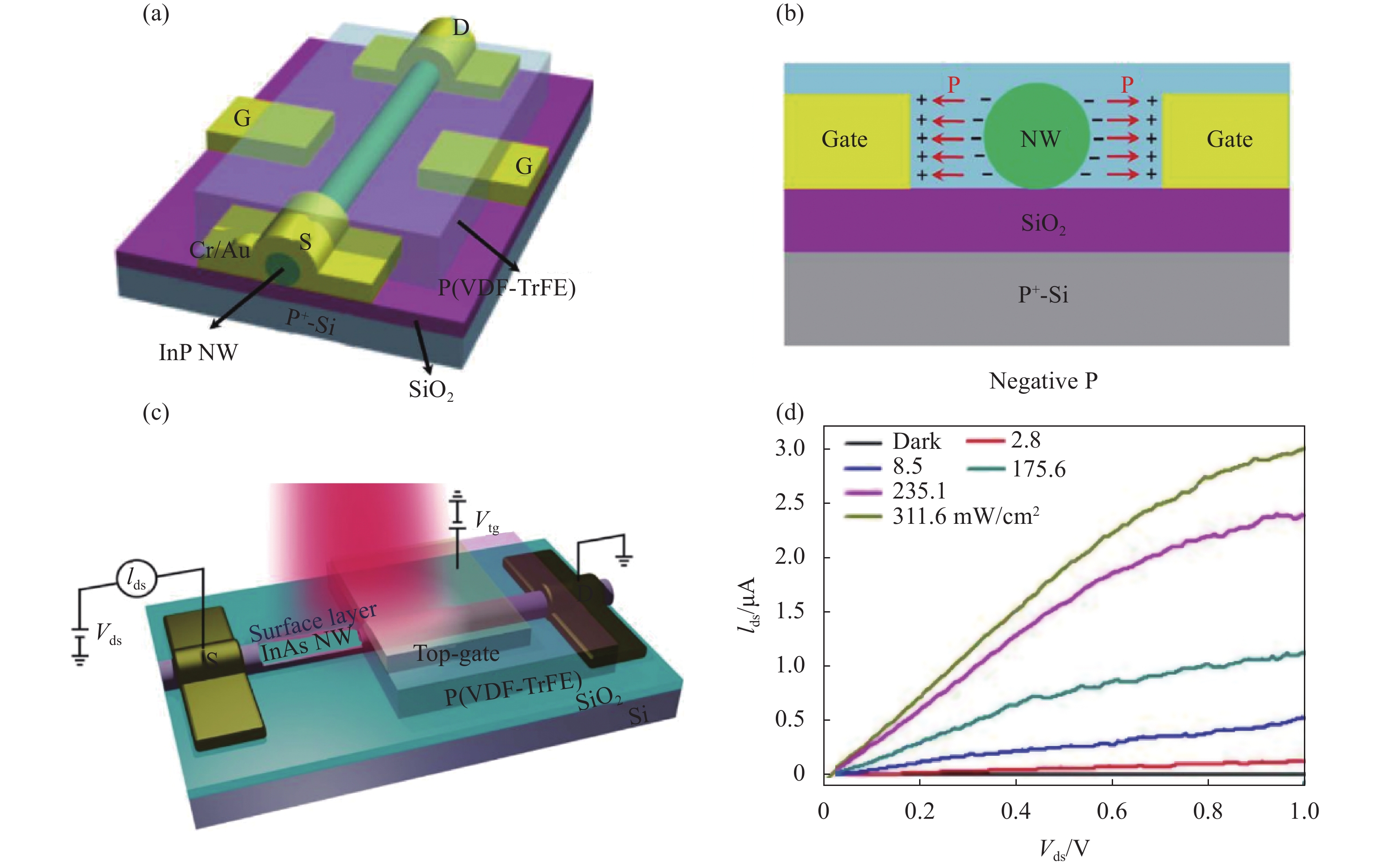
![Ferroelectric localized field-enhanced nanowire photodetectors. (a) Device structure schematic of ferroelectric side-gated single InP NW; (b) Working principle diagram of the device in the negative polarization state[15]; (c) Device structure schematic of ferroelectric top-gated single InAs NW; (d) Output characteristic curves of the device for 3.5 μm exciting light at different power densities[18]](/richHtml/irla/2022/51/7/20220288/img_1.jpg)
Fig. 1. Ferroelectric localized field-enhanced nanowire photodetectors. (a) Device structure schematic of ferroelectric side-gated single InP NW; (b) Working principle diagram of the device in the negative polarization state[15]; (c) Device structure schematic of ferroelectric top-gated single InAs NW; (d) Output characteristic curves of the device for 3.5 μm exciting light at different power densities[18]
![Ferroelectric localized field-enhanced MoS2 photodetector. (a) Schematic diagram of MoS2 top-gate device structure tuned by ferroelectric material; (b) Photoresponsivity under different wavelength[14]; (c) Schematic diagram of structure and test circuit of MoS2 negative capacitance field effect transistor tuned by ferroelectric material; (d) Transfer characteristic curves under different incident light powers[23]](/richHtml/irla/2022/51/7/20220288/img_2.jpg)
Fig. 2. Ferroelectric localized field-enhanced MoS2 photodetector. (a) Schematic diagram of MoS2 top-gate device structure tuned by ferroelectric material; (b) Photoresponsivity under different wavelength[14]; (c) Schematic diagram of structure and test circuit of MoS2 negative capacitance field effect transistor tuned by ferroelectric material; (d) Transfer characteristic curves under different incident light powers[23]
Fig. 3. Ferroelectric localized field-enhanced two-dimensional material photodetectors. (a) Structure schematic of ferroelectric material tuned InSe phototransistor[26]; (b) Structure schematic of ferroelectric material tuned InSb phototransistor[28]
Fig. 4. Modulation of two-dimensional material photodetectors by pyroelectric effect of ferroelectric materials. (a) Schematic diagram of graphene pyroelectric bolometer; (b) Working principle diagram of graphene pyroelectric bolometer[29]; (c) P(VDF-TrFE)/MoS2 field effect transistor structure[30]; (d) Structure schematic of Bi2O2Se/PMN-PT ferroelectric field effect transistor[31]
Fig. 5. Ferroelectric localized field-enhanced two-dimensional material homojunction devices. (a) Schematic diagram of BiFeO3 ferroelectric tuned WSe2 in-plane pn junction; (b) Output characteristics of the device[32]; (c) Schematic diagram of P(VDF-TrFE) ferroelectric tuned MoTe2 in-plane pn junction; (d) Photocurrent mapping of the device[33]
Fig. 6. Ferroelectric localized field-enhanced two-dimensional van der Waals heterojunction devices[35]. (a) Device structure schematic of ferroelectric tuned GeSe/MoS2 heterojunction; (b)-(d) Schematic diagram of the energy band structure of the heterojunction corresponding to the different ferroelectric polarization states

Set citation alerts for the article
Please enter your email address


