
Jia-Lu Zhu, Ren-Chao Jin, Li-Li Tang, Zheng-Gao Dong, Jia-Qi Li, Jin Wang. Multidimensional trapping by dual-focusing cylindrical vector beams with all-silicon metalens[J]. Photonics Research, 2022, 10(5): 1162
- Photonics Research
- Vol. 10, Issue 5, 1162 (2022)
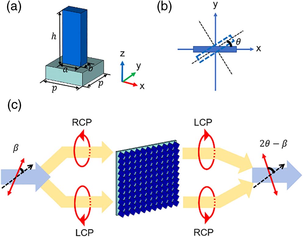
Fig. 1. Schematic of the anisotropic elementary unit and the working principle for the CVB converter. (a) The all-silicon unit configuration consisting of the bar and substrate. (b) The rotation angle θ x x
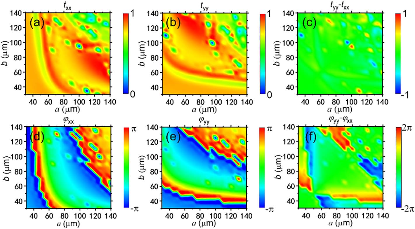
Fig. 2. Simulation of transmission amplitude (t x x t y y φ x x φ y y a b
Fig. 3. Simulated amplitude (t x x t y y ( t y y − t x x ) φ x x φ y y | φ y y − φ x x | 2 π
Fig. 4. Schematic of the transverse dual-focusing CVB system. The inset on the right illustrates the specific arrangement of metasurface elements.
Fig. 5. Simulation results of the transverse dual-focusing CVB system under the incidence of x E x – y z = 1200 μm E x – z y = 0 μm E x – y z = 1200 μm x – y z = 1200 μm
Fig. 6. Schematic of the longitudinal dual-focusing CVB system. The top inset illustrates the arrangement of the bar elements.
Fig. 7. Simulation results of the longitudinal dual-focusing CVB system under the incidence of x E x – y z = 1200 μm f 1 f 2 E x – z y = 0 μm
Fig. 8. Simulation results of the longitudinal polarization-dependent dual-focusing CVB system under the incidence of y E x – y z = 1200 μm f 1 f 2 E f 1 f 2
Fig. 9. Calculation results of the optical force. (a) Schematic of the longitudinal dual-focusing CVB metalens and the glass sphere which is subjected to the optical force. (b) Calculated longitudinal optical force F z f 1 x F x F y f 1 y E

Set citation alerts for the article
Please enter your email address
© Copyright 2018-2021 | Chinese Laser Press. All Rights Reserved 沪ICP备15018463号-20