Zhou Yang, Shengzhong Liu. Perspective on the imaging device based on perovskite materials[J]. Journal of Semiconductors, 2020, 41(5): 050401
Search by keywords or author
- Journal of Semiconductors
- Vol. 41, Issue 5, 050401 (2020)
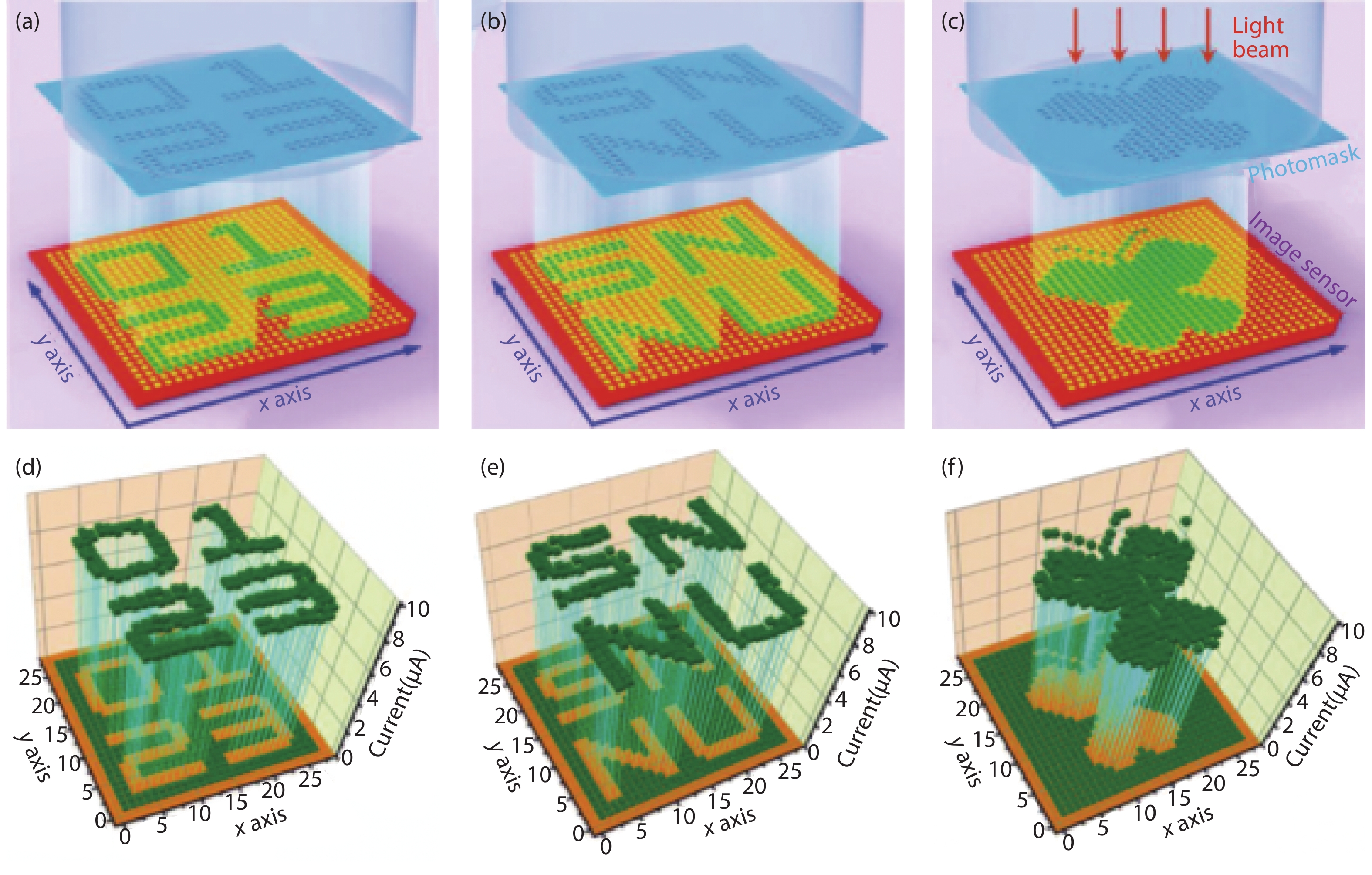
![(Color online) (a)–(c) Schematic illustration for the projection imaging mechanism. A prepatterned photomask was used directly above the imaging assembly. Under light illumination, the optical pattern is projected through the mask with bright and dark contrast to form the image of the mask on the sensor unit. (d)–(f) The corresponding photocurrent outputs from each pixel measured under 2 V bias with different optical patterns of “0123”, “SNNU”, and an image of a butterfly. Reproduced with permission[13]. Copyright 2018, Wiley-VCH.](/richHtml/jos/2020/41/5/050401/img_1.jpg)
Fig. 1. (Color online) (a)–(c) Schematic illustration for the projection imaging mechanism. A prepatterned photomask was used directly above the imaging assembly. Under light illumination, the optical pattern is projected through the mask with bright and dark contrast to form the image of the mask on the sensor unit. (d)–(f) The corresponding photocurrent outputs from each pixel measured under 2 V bias with different optical patterns of “0123”, “SNNU”, and an image of a butterfly. Reproduced with permission[13 ]. Copyright 2018, Wiley-VCH.

Set citation alerts for the article
Please enter your email address


