Large light absorption coefficients, tunable bandgaps, high tolerance to defects, long carrier lifetimes as well as diffusion lengths render lead halide perovskite materials ideal candidates for optoelectronic devices. Except application in solar cell, photodetectors based on perovskite materials have been recognized as another game changer due to the achievements such as high responsivity of 1.9 × 10⁴ A/W[
- Journal of Semiconductors
- Vol. 41, Issue 5, 050401 (2020)
Abstract
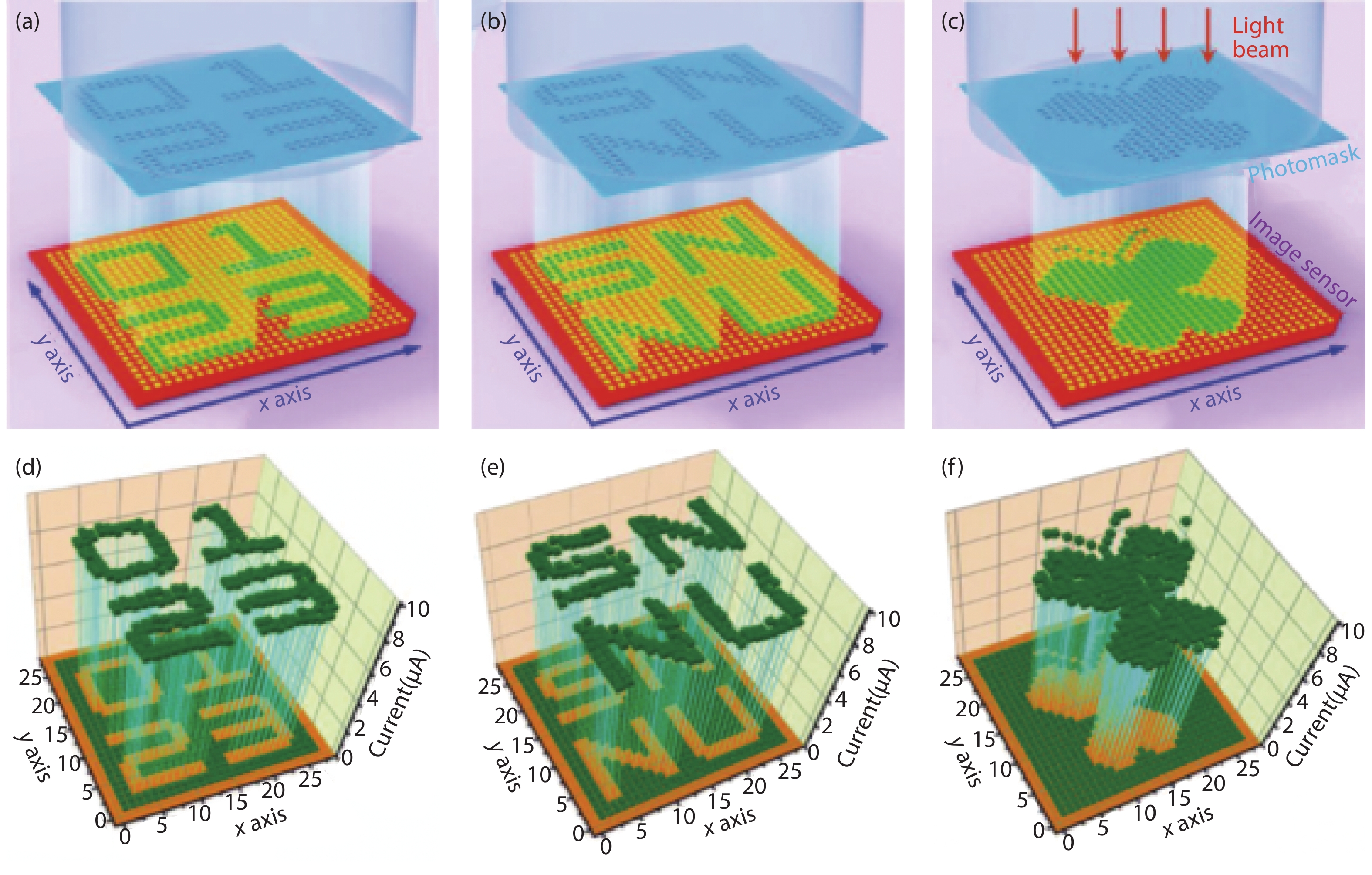
Those advantages have extended to imaging devices, which were achieved by assembling pixel array on perovskite materials (Fig. 1)[
![]()
Figure 1.(Color online) (a)–(c) Schematic illustration for the projection imaging mechanism. A prepatterned photomask was used directly above the imaging assembly. Under light illumination, the optical pattern is projected through the mask with bright and dark contrast to form the image of the mask on the sensor unit. (d)–(f) The corresponding photocurrent outputs from each pixel measured under 2 V bias with different optical patterns of “0123”, “SNNU”, and an image of a butterfly. Reproduced with permission[
The further efforts should be paid on: (1) the design and building of integrating circuit on large size single-crystalline perovskites. Single-crystalline perovskite shows better optoelectronic properties and detection performance than those of poly-crystalline thin films. However, the large-size single-crystalline perovskite is till limited. At the same time, ionic nature of perovskite makes it not compatible with currently used photolithography technology, which is urgent for developing high-resolution imaging sensor. (2) working mechanism of perovskite detector. Perovskite is an ionic and electronic transport. The electrical as well as optical stimulations will affect the transportation as well as distribution of these two kinds of carriers. The better understanding of the complex transportation phenomenon will easy the design and fabrication of high-performance devices. (3) device stability. As well known, perovskite will decompose under the stresses of light, heat, humidity. For detector, the heat and humidity are most important factors affecting its stability and should be concerned during device design and material selection. (4) toxic problem. That is a dilemma accompanying with the development of lead halide perovskite devices. As lead provides very good optoelectronic properties for perovskites, the toxic problem is much concerning during the large-scale application of perovskite materials. Less toxic materials with similar optoelectronic properties are desired.
References
[1] C Chen, g X Q Zhang, u G Wu et al. Visible-light ultrasensitive solution-prepared layered organic-inorganic hybrid perovskite field-effect transistor. Adv Optical Mater, 5, 1600539(2017).
[2] L Dou, Y Yang, J You et al. Solution-processed hybrid perovskite photodetectors with high detectivity. Nat Commun, 5, 5404(2014).
[3] W H Wang, Y R Ma, L M Qi. High-performance photodetectors based on organometal halide perovskite nanonets. Adv Func Mater, 27, 1603653(2017).
[4] L Shen, g Y Fang, g D Wang et al. A self-powered, sub-nanosecond-response solution-processed hybrid perovskite photodetector for time-resolved photoluminescence-lifetime detection. Adv Mater, 28, 10794(2016).
[5] Q Lin, n A Armin, s D M Lyons et al. Low noise, IR-blind organohalide perovskite photodiodes for visible light detection and imaging. Adv Mater, 27, 2060(2015).
[6] Y Fang, g J Huang. Resolving weak light of sub-picowatt per square centimeter by hybrid perovskite photodetectors enabled by noise reduction. Adv Mater, 27, 2804(2015).
[7] Q Lin, n A Armin, n P L Burn et al. Filterless narrowband visible photodetectors. Nat Photonics, 9, 687(2015).
[8] Y J Fang, g Q F Dong, o Y C Shao et al. Highly narrowband perovskite single-crystal photodetectors enabled by surface-charge recombination. Nat Photonics, 9, 679(2015).
[9] S Chen, g C Teng, g M Zhang et al. A flexible UV–Vis–NIR photodetector based on a perovskite/conjugated-polymer composite. Adv Mater, 28, 5969(2016).
[10] X Zheng, o W Zhao, g P Wang et al. Ultrasensitive and stable X-ray detection using zero-dimensional lead-free perovskites. J Energy Chem, 49, 299(2020).
[11] M Hu, a S Jia, u Y Liu et al. Large and dense organic–inorganic hybrid perovskite CH3NH3PbI3 wafer fabricated by one-step reactive direct wafer production with high X-ray sensitivity. ACS Appl Mater Interfaces, 12, 16592(2020).
[12] W Pan, g B Yang, u G Niu et al. Hot-pressed CsPbBr3 quasi-monocrystalline film for sensitive direct X-ray detection. Adv Mater, 31, 1904405(2019).
[13] Y Liu, g Y Zhang, o K Zhao et al. A 1300 mm2 ultrahigh-performance digital imaging assembly using high-quality perovskite single crystals. Adv Mater, 30, 1707314(2018).
[14] Y Zhang, Y Liu, Z Xu et al. Nucleation-controlled growth ofsuperior lead-free perovskite Cs3Bi2I9 single-crystals for high performance X-ray detection. Nat Commun, 11, 2304(2020).
[15] Y C Kim, m K H Kim, n D Y Son et al. Printable organometallic perovskite enables large-area, low-dose X-ray imaging. Nature, 550, 87(2017).

Set citation alerts for the article
Please enter your email address


