• Journal of Semiconductors
  • Vol. 44, Issue 12, 120501 (2023)
Rashid Khan1, Guangyi Shi1, Wenjing Chen1, Zhengguo Xiao1、*, and Liming Ding2、**
Author Affiliations
  • 1Key Laboratory of Strongly-Coupled Quantum Matter Physics (CAS), Department of Physics, University of Science and Technology of China, Hefei 230026, China
  • 2Center for Excellence in Nanoscience (CAS), Key Laboratory of Nanosystem and Hierarchical Fabrication (CAS), National Center for Nanoscience and Technology, Beijing 100190, China
  • show less
    DOI: 10.1088/1674-4926/44/12/120501 Cite this Article
    Rashid Khan, Guangyi Shi, Wenjing Chen, Zhengguo Xiao, Liming Ding. Interface engineering yields efficient perovskite light-emitting diodes[J]. Journal of Semiconductors, 2023, 44(12): 120501 Copy Citation Text show less

    Abstract

    In short, we realized the interface passivation of perovskite films by using a series of alkylammonium iodides with different alkyl chain lengths. Longer alkyl chain favors defects passivation and device performance. The PeLEDs with DAI layer gave an EQE of 16.5%.

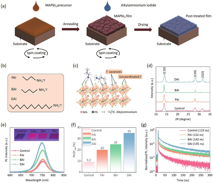
    Afterward, we compared the optoelectronic properties of the control and post-treated perovskite films to evaluate the passivation ability of PAI, BAI, and DAI, respectively. Fig. 1(e) shows the photoluminescence (PL) spectra of the films, showing increase in peak intensity as alkyl chain length increases. The slight blue-shift of PL peaks was observed in the film with post-treatment, which can be attributed to the reduction of defect density for the film[33, 34]. The photo images for the films under UV light can confirm these results (inset of Fig. 1(e)). Furthermore, we conducted the external-photoluminescence quantum yield (PLQYext) and time-resolved photoluminescence (TRPL) measurements to examine the impact of post-treatment on carrier recombination dynamics (Figs. 1(f) and 1(g)). The average carrier lifetime (Taverage) and PLQYext values for the post-treated films increased significantly compared to the control film (Table S1). The control film has a Taverage of 123 ns and a PLQYext of 9.2%, while the films post-treated with PAI, BAI, and DAI showed bigger Taverage values of 152 ns, 142 ns, and 135 ns, respectively. In addition, the PLQYext values for the post-treated films increased substantially, with values of 20%, 25%, and 35% for PAI, BAI, and DAI cases, respectively. We further calculate the radiative (Krad) and non-radiative (Knonrad) recombination rates by using the equation 1Taverage=Krad+Knonrad and PLQYext=KradKrad+Knonrad. The Knonrad value reduced from 7.3 × 10⁶ s−1 for the control film to 4.8 × 10⁶ s−1 for DAI-treated film (Table S1). This reduction of the non-radiative recombination losses indicates that the alkylammonium iodides with longer chain reduce more surface defects[25, 35].

    Metal-halide perovskites (MHPs) have emerged as a new class of semiconductors used in perovskite solar cells (PSCs)[15], perovskite light-emitting diodes (PeLEDs)[612], photo/X-ray detectors[1316], and memristors[17, 18]. PeLEDs can emit different light with high purity[19, 20]. Over the past few years, the external quantum efficiency (EQE) has been rapidly increased from less than 1% to above 28% due to the intensive research efforts in composition engineering, device structure optimization and defect passivation[2123]. Interface defects passivation is useful for developing efficient and stable PeLEDs[24]. Alkylammonium salts exhibited strong passivation function due to the chemical interaction between ammonium and [PbI6]4− octahedron[25, 26]. The alkyl chain length is a critical factor in defect passivation[27], which has been demonstrated in perovskite solar cells[28]. In this work, we thoroughly examined the functions of alkylammonium iodide with tunable alkyl chain lengths (propyl ammonium iodide (PAI), butylammonium iodide (BAI), and dodecylammonium iodide (DAI)) in passivating defects of the interface between MAPbI3 emission layer and the electron-transport layer (ETL). We found that the passivation function intensifies with increasing alkyl chain length. The EQE reaches 16.5% when the emissive layer is post-treated by DAI with longer chain.

    (Color online) (a) Fabrication of MAPbI3 films and post-treatments with alkylammonium iodides. (b) Chemical structures for ammonium salts. (c) Surface defects passivation with alkylammonium iodides. (d) XRD profiles for perovskite films before and after post-treatments. (e) PL spectra. Inset: perovskite films under UV light. (f) PLQYext. (g) TRPL analysis for the control and post-treated perovskite films.

    Figure 1.(Color online) (a) Fabrication of MAPbI3 films and post-treatments with alkylammonium iodides. (b) Chemical structures for ammonium salts. (c) Surface defects passivation with alkylammonium iodides. (d) XRD profiles for perovskite films before and after post-treatments. (e) PL spectra. Inset: perovskite films under UV light. (f) PLQYext. (g) TRPL analysis for the control and post-treated perovskite films.

    The improved optical properties for MAPbI3 films with post-treatment enable us to fabricate efficient PeLEDs. The device structure with post-treatments is shown in Fig. 2(a). To determine the ideal concentration of alkylammonium iodides, we made PeLEDs with post-treatments by using different concentrations of DAI. A DAI concentration of 10 mg/ml led to a higher EQE. Therefore, we fixed the concentration of alkylammonium iodides at 10 mg/ml for post-treatments (Fig. 2(b)). Figs. 2(c) and 2(d) show the JV and EQE curves of PeLEDs. The EQE increases dramatically from 3.3% (control) to 4.2% (PAI), 8.9% (BAI), and 16.5% (DAI). The EQE for DAI case is the highest. The EQE statistics based on 10 devices show very small variations, indicating good repeatability (Fig. 2(e)). Fig. 2(f) shows the electroluminescence (EL) spectra for control device and post-treated devices, being consistent with PL spectra.

    Fig. 1(b) depicts the chemical structures of alkylammonium iodides, which consist of the same end groups but different alkyl chains. Fig. 1(c) illustrates the alkylammonium-passivated perovskite lattice. The alkylammonium iodides coated on the perovskite layer fill the iodine vacancies and passivate uncoordinated iodine defects on the surface through ionic and hydrogen bonding[25, 26]. X-ray diffraction (XRD) results show no additional diffraction peaks after post-treatment (Fig. 1(d)). The scanning electron microscopy (SEM) images for the perovskite films also exhibit negligible differences in surface morphology before and after post-treatment (Fig. S1). Those little change in lattice structure and grain size after surface treatment indicate no grain growth or dissolution by post-treatment.

    (Color online) (a) The device structure. (b) EQE statistics for PeLEDs with post-treated films by using DAI solutions with different concentrations. (c) J−V curves. (d) EQE vs current density curves. (e) EQE statistics. (f) EL spectra for PeLEDs without and with post-treatments.

    Figure 2.(Color online) (a) The device structure. (b) EQE statistics for PeLEDs with post-treated films by using DAI solutions with different concentrations. (c) J−V curves. (d) EQE vs current density curves. (e) EQE statistics. (f) EL spectra for PeLEDs without and with post-treatments.

    MAPbI3 film fabrication and subsequent post-treatment are shown in Fig. 1(a). Because of the low-temperature synthesis and crystallographic features of perovskite, numerous defect sites, especially I defects and delocalized organic amine defects, exist on perovskite film surface and grain boundaries[2932]. These defect sites act as the recombination centers, limiting the device performance. To passivate these defects, the perovskite layer was post-treated by spin-coating a thin layer of alkylammonium salt, then followed by heating.

    References

    [1] A Kojima, K Teshima, Y Shirai et al. Organometal halide perovskites as visible-light sensitizers for photovoltaic cells. J Am Chem Soc, 131, 6050(2009).

    [2] M A Green, A Ho-Baillie, H J Snaith. The emergence of perovskite solar cells. Nat Photonics, 8, 506(2014).

    [3] Z G Xiao, Y B Yuan, Q Wang et al. Thin-film semiconductor perspective of organometal trihalide perovskite materials for high-efficiency solar cells. Mater Sci Eng R Rep, 101, 1(2016).

    [4] H Min, D Y Lee, J Kim et al. Perovskite solar cells with atomically coherent interlayers on SnO2 electrodes. Nature, 598, 444(2021).

    [5] S Zhang, F Y Ye, X Y Wang et al. Minimizing buried interfacial defects for efficient inverted perovskite solar cells. Science, 380, 404(2023).

    [6] Z K Tan, R S Moghaddam, M L Lai et al. Bright light-emitting diodes based on organometal halide perovskite. Nat Nanotechnol, 9, 687(2014).

    [7] Z G Xiao, R A Kerner, L F Zhao et al. Efficient perovskite light-emitting diodes featuring nanometre-sized crystallites. Nat Photonics, 11, 108(2017).

    [8] J Chen, P C Ma, W J Chen et al. Overcoming outcoupling limit in perovskite light-emitting diodes with enhanced photon recycling. Nano Lett, 21, 8426(2021).

    [9] G Q Cheng, Y Liu, T Chen et al. Efficient all-inorganic perovskite light-emitting diodes with improved operation stability. ACS Appl Mater Interfaces, 12, 18084(2020).

    [10] D Ye, Z J Li, W J Chen et al. Stable yellow light-emitting diodes based on quasi-two-dimensional perovskites. ACS Appl Mater Interfaces, 14, 34918(2022).

    [11] X K Liu, W D Xu, S Bai et al. Metal halide perovskites for light-emitting diodes. Nat Mater, 20, 10(2021).

    [12] R Khan, S L Chu, Z J Li et al. High radiance of perovskite light-emitting diodes enabled by perovskite heterojunctions. Adv Funct Mater, 32, 2203650(2022).

    [13] L T Dou, Y Yang, J B You et al. Solution-processed hybrid perovskite photodetectors with high detectivity. Nat Commun, 5, 5404(2014).

    [14] S Yakunin, M Sytnyk, D Kriegner et al. Detection of X-ray photons by solution-processed lead halide perovskites. Nat Photonics, 9, 444(2015).

    [15] H T Wei, Y J Fang, P Mulligan et al. Sensitive X-ray detectors made of methylammonium lead tribromide perovskite single crystals. Nat Photonics, 10, 333(2016).

    [16] Q S Chen, J Wu, X Y Ou et al. All-inorganic perovskite nanocrystal scintillators. Nature, 561, 88(2018).

    [17] Z G Xiao, Y B Yuan, Y C Shao et al. Giant switchable photovoltaic effect in organometal trihalide perovskite devices. Nat Mater, 14, 193(2015).

    [18] Z G Xiao, J S Huang. J Energy-efficient hybrid perovskite memristors and synaptic devices. Adv Electron Mater, 2, 1600100(2016).

    [19] Z Fang, W Chen, Y Shi et al. Dual passivation of perovskite defects for light-emitting diodes with external quantum efficiency exceeding 20%. Adv Funct Mater, 30, 1909754(2020).

    [20] V D’Innocenzo, A R Srimath Kandada, M De Bastiani et al. Tuning the light emission properties by band gap engineering in hybrid lead halide perovskite. J Am Chem Soc, 136, 17730(2014).

    [21] Z Liu, W D Qiu, X M Peng et al. Perovskite light-emitting diodes with EQE exceeding 28% through a synergetic dual-additive strategy for defect passivation and nanostructure regulation. Adv Mater, 33, 2103268(2021).

    [22] J S Kim, J M Heo, G S Park et al. Ultra-bright, efficient and stable perovskite light-emitting diodes. Nature, 611, 688(2022).

    [23] W H Bai, T T Xuan, H Y Zhao et al. Perovskite light-emitting diodes with an external quantum efficiency exceeding 30%. Adv Mater, 35, 2302283(2023).

    [24] Y W Guo, S Apergi, N Li et al. Phenylalkylammonium passivation enables perovskite light emitting diodes with record high-radiance operational lifetime: The chain length matters. Nat Commun, 12, 644(2021).

    [25] H Kim, S U Lee, D Y Lee et al. Optimal interfacial engineering with different length of alkylammonium halide for efficient and stable perovskite solar cells. Adv Energy Mater, 9, 1902740(2019).

    [26] X F Ye, H K Cai, Q H Sun et al. Alkyl ammonium salt with different chain length for high-efficiency and good-stability 2D/3D hybrid perovskite solar cells. Org Electron, 106, 106542(2022).

    [27] W H Feng, C X Zhang, J X Zhong et al. Correlating alkyl chain length with defect passivation efficacy in perovskite solar cells. Chem Comm, 56, 5006(2020).

    [28] P J Zhao, J Subbiah, B L Zhang et al. Alkyl chain length-dependent amine-induced crystallization for efficient interface passivation of perovskite solar cells. Adv Mater Interfaces, 10, 2202313(2023).

    [29] H Na, Q L Meng, J Cha et al. Passivating detrimental grain boundaries in perovskite films with strongly interacting polymer for achieving high-efficiency and stable perovskite solar cells. Appl Surf Sci, 626, 157209(2023).

    [30] F Wang, S Bai, W Tress et al. Defects engineering for high-performance perovskite solar cells. NPJ Flex Electron, 2, 22(2018).

    [31] T S Sherkar, C Momblona, L Gil-Escrig et al. Recombination in perovskite solar cells: Significance of grain boundaries, interface traps, and defect ions. ACS Energy Lett, 2, 1214(2017).

    [32] X Y Shen, K Kang, Z K Yu et al. Passivation strategies for mitigating defect challenges in halide perovskite light-emitting diodes. Joule, 7, 272(2023).

    [33] Z Liu, K Meng, X Wang et al. In situ observation of vapor-assisted 2D-3D heterostructure formation for stable and efficient perovskite solar cells. Nano Lett, 20, 1296(2020).

    [34] Y C Shao, Z G Xiao, C Bi et al. Origin and elimination of photocurrent hysteresis by fullerene passivation in CH3NH3PbI3 planar heterojunction solar cells. Nat Commun, 5, 5784(2014).

    [35] B P Kore, W Zhang, B W Hoogendoorn et al. Moisture tolerant solar cells by encapsulating 3D perovskite with long-chain alkylammonium cation-based 2D perovskite. Commun Mater, 2, 100(2021).

    Rashid Khan, Guangyi Shi, Wenjing Chen, Zhengguo Xiao, Liming Ding. Interface engineering yields efficient perovskite light-emitting diodes[J]. Journal of Semiconductors, 2023, 44(12): 120501
    Download Citation