
Yonggang Yan, Zhengxing Wu, Zhi Li, Yuqi Tang. Traceable analysis of the performance of an ultra-fine positioning stage using a differential plane mirror interferometer[J]. Infrared and Laser Engineering, 2021, 50(11): 20210070
- Infrared and Laser Engineering
- Vol. 50, Issue 11, 20210070 (2021)
Abstract
0 Introduction
Developments in precision manufacturing, piezoelectric material processing, position-sensing and control system, have increased the demand for ultrahigh precision micro- and nano-positioning stages with pico-meter displacement resolution. Such stages are the indispensable components of industrial and metrological instruments, precision measurement, nano-technology, and advanced material analysis[
Commercial SPMs are able to determine the thickness of a single or few layer two-dimensional materials with an accuracy of better than 0.1 nm[
Recent applications in nanotechnology require that not only the nanopositioning of the commercial stages have to be based on precise measurements but the traceability of the measuring technique has to be ensured up to the primary standard. Traceable measurements of the nanopositioning stages are classified as both main configurations of laser interferometers: homodyne and heterodyne. The former setup uses a single frequency laser source and exhibits high measurement accuracy. The latter is of larger nonlinearity because of the errors caused by frequency and polarization mixing[
In this work, a reliable calibration method and system for traceable performance evaluation of ultra-fine stage is realized using a differential plane mirror interferometer from NPL, the magnitude of the cyclic error of which is ±20 pm[
1 Proposed method and system configuration
A reliable calibration method for the investigation of the quasi-static performances for nano-positioning stage is proposed and the corresponding system is developed, which consists of an optical system based on a differential plane mirror interferometer with double-pass configuration from NPL[
By means of the different plane mirror interferometer, the movement displacement of the ultra-fine positioning stage can be transmitted to the phases of the photoelectric signals. The variation of the signals is acquired by the data acquisition and decoding system, and the displacement is calculated successfully. On the base, the method and its system can be used to calibrate and trace the metrological characteristics of nano-positioning stages effectively and creatively.
1.1 Optical system
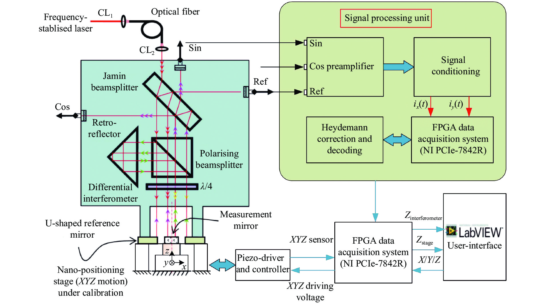
The optical configuration of the NPL Jamin Differential Plane Mirror interferometer is shown as Fig.1. The interferometer based on a common-path optical configuration is regarded as a standard. The laser beam (λ=632.991 nm) coming from a frequency-stabilized He-Ne laser (Thorlabs, intensity stabilization of ±0.2%) is firstly coupled into a polarization-maintaining single-mode (PM) fiber through Faraday optical isolator and aperture, and then delivered to the integrated interferometric calibration system, thereby separating the heat generated by the laser from the experimental devices. This optical fiber delivery system has also effectively decoupled the laser source from the calibration setup, and therefore offered flexibility for the following calibration work.
![]()
Figure 1.Traceable calibration layout for quality control of micro-/nano-positioining stages
The decoupled laser beam enters the Jamin interferometer after it is collimated by an aspheric lens, and forms the linearly reference and measurement laser beams. Then they are reflected back from the U-shaped reference and measurement mirror respectively to produce an interference pattern incident.
Owing to the phase quadrature coatings at the corresponding positions on the Jamin beamsplitter, two phase-quadrature interference signals (sin and cos, in Fig.1) are generated and captured by the photo detectors, given as the optimum signal-to-noise conditions for fringe counting and subdividing.
While the moving measurement mirror travels attached to an ultra-fine stage which is driven by a piezoelectric actuator, its relative displacement can be expressed in Eq.(1):
where N is the number of the interferometric fringe, and λ is the wavelength of the frequency-stabilized He-Ne laser beam.
1.2 Mechanical system
A mechanical system of the calibration setup has been fabricated correctly to be in accordance with the design and configuration of the NPL interferometer. The interferometer block together with its U-shaped reference mirror is supported by three evenly-distributed columns made of invar. Two micrometers located on the V-groove of the invar columns (not shown in Fig.1) are used to align the measurement beams with the measurement mirror, which is fixed onto the stage under calibration. Three additional micrometers are utilized for fine adjustment of the U-shaped reference mirror. Care has been taken to make sure that (1) the reference mirror is vertical to the reference beams, (2) the optical path difference between the reference and the measurement beams is close to zero, and (3) the calibrated setup should be let stand still for 72 h after the adjustment and tight fixation.
1.3 Data acquisition and signal processing
The phase quadrature interference signals (sin and cos, shown in Fig.1) together with the reference signal are firstly transmitted into a NPL-developed preamplifier for current-to-voltage conversion, amplification and denoising. The signals are then processed using a NPL-developed signal optimizing unit to remove the direct current (DC) offset of the signals, compensate for the potential laser intensity fluctuation, and amplify the analog signals in such a way that they can match with the full dynamic range of the analog to digital converters (ADCs) on the field-programmable gate array (FPGA) card. The magnified quadrature interference signals ix(t) and iy(t), acquired from the signal conditioning unit have nearly zero-offset, and a magnitude of about ±9 V. And they are converted into a displacement through fringe counting and subdividing.
The two signals ix(t) and iy(t) can be expressed in Eq.(2):
where ix0 and iy0 are the DC offsets; Cx and Cy are the different AC amplitudes for the signal, and φ0 is the phase-quadrature error between the two signals.
In the case of zero-path difference, the displacement ∆L of the measurement mirror is proportional to the phase shift ∆φ in interference signals during the period of [t0, t1], which can be expressed in Equation (5):
where λ is the laser wavelength.
Subsequently, a FPGA-based DAQ system (NI PCIe-7842R) is used to acquire the optimized interference signals ix(t) and iy(t). This multifunction reconfigurable DAQ system features a sampling rate of 200 kS/s with a user programmable FPGA for high-performance onboard signal processing and direct control over I/O signals. This DAQ system is also capable of A/D conversion per channel (16 bit single-ended) for independent timing and triggering. It is therefore especially suitable for high-speed acquisition of phase-quadrature interference signals without introduction of additional phase shifts or retardation between the two signals ix(t) and iy(t).
The digitized interference signals read by this DAQ system are firstly normalized using the Heydemann correction to compensate for the five parameters such as offsets, gains, and signal phase [ix0, iy0,Cx, Cy, φ][
1.4 Quasi-static performance test results of the calibration setup
The interferometric calibration setup is mounted on an optical vibration isolation platform, and works under nearly open-air conditions, as shown in Fig.2. More care is taken that a plastic cover is used to isolate the heat generated by the laser from the experimental devices or other heat source so as to eliminate the influence to the calibrated ultra-fine stage.
![]()
Figure 2.Interferometric calibration setup
Figrue 3(a) shows the mid-term stability and drift of the interferometer within 50 s, which is a typical duration for one nanoindentation process including loading, holding and unloading procedures, respectively.
![]()
Figure 3.Experimental investigation of the quasi-static performance of the interferometric calibration setup
The corresponding noise spectrum density, obtained by using short-time Fourier transform with Hanning window, is illustrated in Fig.3(b). The vertical and horizontal coordinates in this figure are of logarithmic forms. It can be seen from Fig.3 that the calibration setup has a drift smaller than 200 pm within the period of 50 s, and a noise floor lower than 10
To evaluate the relative position and orientation between the optical axis of the interferometer and the measurement mirror mounted onto the z axis of the piezostage within the z-axis motion range, an experiment was carried out under nearly open-air conditions. The z-axis motion deviations of the interferometric calibration setup are measured, and a polynomial fitting is done using least square estimation, as shown in Fig.4.
![]()
Figure 4.Experimental investigation of the
Seen from Fig.4, the interferometric measurement errors are of non-linear with the displacement over the range, and obviously there exists angular variation between the optical axis of the interferometer and the measurement mirror due to possible temperature fluctuation. They may be also caused by other reasons such as the near heat, surface shape error of the mirror, the interference intensity, and so on. Here, the relative position and orientation between the interferometer and the piezostage is adjusted again till there exists less angular error between the optical axis and the measurement mirror. So, it can be evaluated that the performance of the interferometric calibration setup can be further improved when the setup is located in a well air-conditioned measurement box with additional heatproof and vibration isolation.
2 Calibration results for a piezostage
A pico-positioning stage (Nano-met3) with good positioning resolution in the picometer range, which will be used in PTB for nanoindentation with indentation depths down to a few picometers or large-range scanning probe microscopes, has been characterized using the proposed calibration setup. This stage has a displacement range of 5 μm in the z-axis direction, and has individually a displacement range of 75 μm in the x-axis/y-axis direction. For the purpose of quasi-static calibration of the direct current performance of this stage, three of the analog outputs (AOs) on the DAQ system are used to drive the stage with a user-programmable LabView software.
In the case of our calibration setup, the FPGA-based DAQ system has a resolution of 0.305 mV (Vp−p=20 V), yielding the resolution for displacement sensing with this approach to be about 170 pm. The displacements of the ultra-fine positioning stage are simultaneously measured using its built-in PicoQ® sensors and the interferometric calibration setup.
2.1 Linear calibration
After the stabilization of 24 h, the experiment is carried on in closed-loop mode of the piezostage and under nearly open-air condition (in plastic cover). The stage is driven in the forward and backward direction during the experiment. And the acquired data for the interferometer and the piezostage are filtered, and fitted linearly using least square estimate. Figure 5 shows the linear error within the full-scale range, and the maximum error is 0.61 nm. Then, the linearity is calculated approximately to be 1.2×10⁻⁴.
![]()
Figure 5.Interferometric calibration of a piezostage working in closed-loop mode
To investigate the performance of the stage in open-loop mode, another experiment is carried out under the same conditions. Due to the hysteresis effect of piezoestage, the data over the range of 1000 nm are cut out of the full range and processed, as shown in Fig.6.
![]()
Figure 6.Interferometric calibration of a piezostage working in open-loop mode
It can be seen that the error variation is larger with the increasing displacement, and the stage under calibration has a variation of ±1.8 nm. According to the sensibility of the piezostage, it has an open-loop DC response of 639.4 pm/mV.
2.2 Resolution test
To assure the resolution of the nanostage under nearly open-air condition, a voltage output with 20 bit DAC is used to drive the nanostage. A 40 picometer amplitude pulse wave was performed using the 20 bit DAC in the user-programmable LabView software while the built-in sensor with a 24 bit ADC and the interferometer were respectively and simultaneously used to measure the displacement of the nanostage. Figure 7 is the calibration result of the resolution of the nanostage using the proposed interferometric calibration setup.
![]()
Figure 7.Closed-loop displacement of the piezostage measured by the integrated PicoQ® Sensor and the interferometer, respectively
Seen from Fig.7, the resolution of the piezostage can be calibrated with the NPL interferometer and can be up to at least 40 picometer. It indicates that the stage can provide a high-resolution driving displacement for MEMS technology.
2.3 Repeatability test
A pulse wave with the amplitude 2 000 nm was performed to drive the nanostage in the user's LabView software. The interval between the pulse signals was set to be 1 s. Then the initial position and the relative displacement of the calibrated piezostage were measured respectively using the interferometric setup and its built-in sensors. Figure 8 shows the interferometric calibration for repea-tability of the piezostage at the modulated frequency of 400 Hz. It can be seen from Fig.8 that the initial interferometric positioning error is less than 100 pm. So, the initial position is deemed to be identical. Computed the deviation of the amplitudes of the two signals, the displacement repeatability error is within 0.65 nm, and the standard deviation is above 0.2 nm. It indicates that the piezostage has a good repeatability and a strong stability in short time.
![]()
Figure 8.Interferometric calibration for repeatability of the piezostage
3 Conclusion
In this study, a traceable calibration methodology and system for the quantitative investigation of the quasi-static performance of ultra-fine positioning stage has been proposed and realized using the NPL differential plane mirror interferometer and the FPGA-based DAQ. In the case of quasi-static measurements, the interferometric displacement calibration setup under nearly open-air conditions has a resolution of 20 pm for a bandwidth of 1 Hz and a noise floor better than 10
References
[1] Yanhao Dong, Hongbing Yang, Lin Zhang, et al. Ultra‐uniform nanocrystalline materials via two‐step sintering. Advanced Functional Materials, 31, 2007750(2020).
[2] Chunguang Hu, Ridong Zha, Qiuyu Ling, et al. Super-resolution microscopy applications and development in living cell. Infrared and Laser Engineering, 46, 1103002(2017).
[3] Chenhui Du, Liang Gong, Xiaoyong Cai, et al. Micro-nanometer scale vibration in imaging of metrological scanning electron microscope. Optics and Precision Engineering, 27, 860-867(2019).
[4] Ziruo Wu, Yanni Cai, Xingrui Wang, et al. Investigation of AFM tip characterization based on multilayer gratings. Infrared and Laser Engineering, 49, 0213001(2020).
[5] C J Shearer, A D Slattery, A J Stapleton, et al. Accurate thickness measurement of graphene. Nanotechnology, 27, 125704(2016).
[6] A Yacoot, L Koenders, H Wolff. An atomic force microscope for the study of the effects of tip-sample interactions on dimensional metrology. Meas Sci Technol, 18, 350-359(2007).
[7] Zhi Li, Uwe Br, Helmut Wolff, et al. Broadb interferometric acterisation of nanopositioning stages with sub10 pm resolution[C]Proc SPIE, Optical Measurement Systems f Industrial Inspection X, 2017, 10329: 1032944.
[8] Tomasz Podzorny, Grzegorz Budzyń, J Rzepka. Linearization methods of laser interferometers for pico/nano positioning stages. Optik-International Journal for Light and Electron Optics, 124, 6345-6348(2013).
[9] C M Wu, C S Su. Nonlinearity in measurements of length by optical interferometry. Meas Sci Technol, 7, 62-68(1995).
[10] A Yacoot, M Dows. The use of X-ray interferometry to investigate the linearity of the NPL plane mirror differential optical interferometer. Meas Sci Technolo, 11, 1126-1130(2000).
[11] Zhaoli Zeng, Shulian Zhang. Nanometrology technology in precision measurement. Journal of Applied Optics, 33, 846-854(2012).
[12] Minhao Zhu, Xuejian Wu, Haoyun Wei, et al. Closed-loop displacement control system for piezoelectric transducer based on optical frequency comb. Acta Phys Sin, 62, 070702(2013).
[13] L A Haroutunyan, M K Balyan. X-Ray on-axis Fresnel holography using three-block Fresnel zone plate interferometer. Journal of Contemporary Physics (Armenian Academy of Sciences), 55, 248-253(2020).
[14] M J Downs, J W Nunn. Verification of the sub-nanometric capability of an NPL differential plane mirror interferometer with a capacitance probe. Meas Sci Technol, 9, 1437-1440(1998).
[15] P L M Heydemann. Determination and correction of quadrature fringe measurement errors in interferometers. Appl Opt, 20, 3382-3384(1981).


Set citation alerts for the article
Please enter your email address

© Copyright 2018-2021 | Chinese Laser Press. All Rights Reserved 沪ICP备15018463号-20