
Zhiyong Jin, Heming Huang, Yueguang Zhou, Shiyuan Zhao, Shihao Ding, Cheng Wang, Yong Yao, Xiaochuan Xu, Frédéric Grillot, Jianan Duan, "Reflection sensitivity of dual-state quantum dot lasers," Photonics Res. 11, 1713 (2023)
- Photonics Research
- Vol. 11, Issue 10, 1713 (2023)
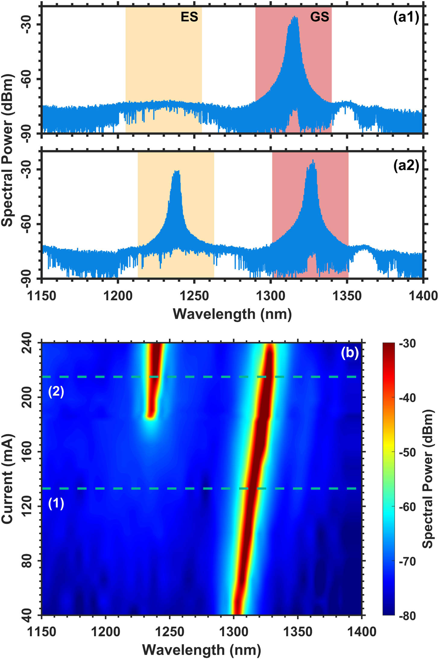
Fig. 1. Optical spectrum of (a1) sole GS lasing and (a2) dual-state lasing of QD lasers. (b) Optical spectrum mapping with the increase of bias current for the dual-state QD laser. Dashed lines (1) and (2) in (b) mark the bias currents of (a1) and (a2), respectively.
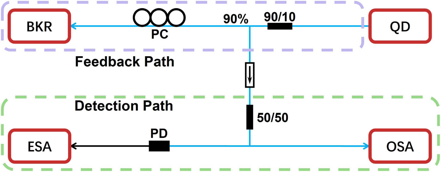
Fig. 2. Experimental setup for investigating the feedback sensitivity of QD lasers. BKR, backreflector; PC, polarization controller; OSA, optical spectrum analyzer; PD, photodiode; ESA, electrical spectrum analyzer.
Fig. 3. Optical (column 1) and RF (column 2) spectrum mappings for QD laser operating at (a) 0.72 × 1 × 1.25 × I th ES
Fig. 4. (a) Optical and (b) RF spectra of QD lasers operated at 1 × I th ES − 9.9 dB − 29 dB
Fig. 5. Schematic representation of the electronic structure and carrier dynamics of QD lasers under optical feedback.
Fig. 6. GS threshold current, ES threshold current, and corresponding ES-GS threshold ratio with respect to ES-GS energy separation.
Fig. 7. Samples of the bifurcation diagrams (column 1), time series (column 2), and GS phase portraits (column 3). (a) Δ E GS ES = 65 meV I / I th ES = 1.0 f ext = − 12.0 dB Δ E GS ES = 80 meV I / I th ES = 1.31 f ext = − 11.0 dB Δ E GS ES = 110 meV I / I th ES = 0.87 f ext = − 13.0 dB f ext r crit
Fig. 8. Critical feedback levels as a function of normalized bias currents (I / I th ES
Fig. 9. Linewidth enhancement factor as a function of normalized bias currents (I / I th ES
Fig. 10. Damping factor and relaxation oscillation frequency versus normalized bias currents (I / I th ES
|
Table 1. Parameters Used in the Simulation


Set citation alerts for the article
Please enter your email address

© Copyright 2018-2021 | Chinese Laser Press. All Rights Reserved 沪ICP备15018463号-20