
Yan Zhang, Mengfan Li, Deyuan Chen. Design and Optimization of Half-Adder Based on Two-Dimensional Photonic Crystal[J]. Laser & Optoelectronics Progress, 2022, 59(1): 0123001
- Laser & Optoelectronics Progress
- Vol. 59, Issue 1, 0123001 (2022)
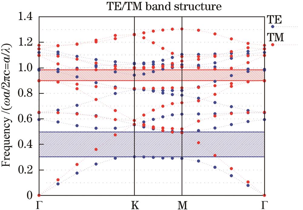
Fig. 1. Energy band diagram of complete photonic crystal structure
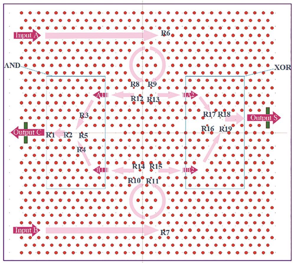
Fig. 2. Structure diagram of half-adder based on AND and XOR logic gates
Fig. 3. TE mode steady-state field distribution of half-adder. (a) A∶0, B∶1; (b) A∶1, B∶0; (c) A∶B∶1
Fig. 4. Time-domain steady state response diagrams of half-adder. (a) A∶0, B∶1; (b) A∶1, B∶0; (c) A∶B∶1
Fig. 5. Structure diagram of the optimized half-adder
Fig. 6. TE mode steady-state field distribution of structure-optimized half-adder. (a) A∶0, B∶1; (b) A∶1, B∶0; (c) A∶B∶1
Fig. 7. Time-domain steady state response diagrams of structure-optimized half-adder. (a) A∶0, B∶1; (b) A∶1, B∶0; (c) A∶B∶1
| ||||||||||||||||||||||||||||||||||||||||||||||||||||||||||||||||||
Table 1. Performance accuracy table and the output power levels of the half-adder designed
| ||||||||||||||||||||||||||||||||||||||||||||||||||||||||||||||||||
Table 2. Performance accuracy table and the output power levels of structure-optimized half-adder

Set citation alerts for the article
Please enter your email address
© Copyright 2018-2021 | Chinese Laser Press. All Rights Reserved 沪ICP备15018463号-20