
Xiaowei Jiang. Broadband absorption of graphene from magnetic dipole resonances in hybrid nanostructure[J]. Journal of Semiconductors, 2019, 40(6): 062006
- Journal of Semiconductors
- Vol. 40, Issue 6, 062006 (2019)
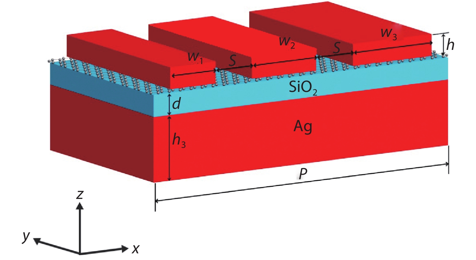
Fig. 1. (Color online) The proposed hybrid nanostructure to broaden graphene absorption bandwidth.
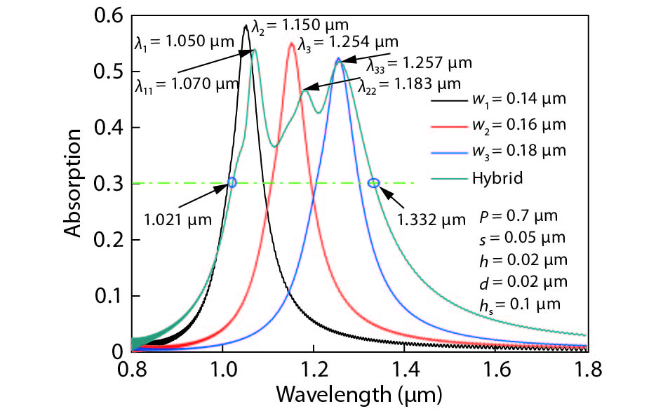
Fig. 2. (Color online) The absorption spectra of monolayer graphene in the wavelength range from 0.8 to 1.8 μ m under normal incidence. Structure parameters: P = 0.7 μ m, s = 0.05 μ m, h = 0.02 μ m, d = 0.02 μ m, h s = 0.1 μ m.
Fig. 3. (Color online) Distribution of magnetic field at different resonance wavelengths on the xoz plane. Structure parameters: P = 0.7 μ m, s = 0.05 μ m, h = 0.02 μ m, d = 0.02 μ m, h s = 0.1 μ m.
Fig. 4. (Color online) Effect of grating width on absorption peaks. Structure parameters: P = 0.7 μ m, s = 0.05 μ m, h = 0.02 μ m, d = 0.02 μ m, h s = 0.1 μ m.
Fig. 5. (Color online) Effect of SiO2 spacer thickness on absorption peaks. Structure parameters: P = 0.7 μ m, s = 0.05 μ m, h = 0.02 μ m, h s = 0.1 μ m, w 1 = 0.14 μ m, w 2 = 0.16 μ m, w 3 = 0.18 μ m.
Fig. 6. (Color online) Effect of grating spacing on absorption peaks. Structure parameters: P = 0.7 μ m, d = 0.02 μ m, h = 0.02 μ m, h s = 0.1 μ m, w 1 = 0.14 μ m, w 2 = 0.16 μ m, w 3 = 0.18 μ m.

Set citation alerts for the article
Please enter your email address
© Copyright 2018-2021 | Chinese Laser Press. All Rights Reserved 沪ICP备15018463号-20