
Xiaowei Jiang. Broadband absorption of graphene from magnetic dipole resonances in hybrid nanostructure[J]. Journal of Semiconductors, 2019, 40(6): 062006
- Journal of Semiconductors
- Vol. 40, Issue 6, 062006 (2019)
Abstract
1. Introduction
Graphene is a two-dimensional (2D) carbon sheet with a honeycomb lattice[
In order to improve monolayer graphene absorption efficiency, several physical mechanisms have been proposed including one-dimensional photonic crystals[
In this letter, we propose a novel hybrid nanostructure and numerically demonstrate the graphene absorption efficiency over 30% and absorption bandwidth more than 0.3 μm in near-infrared region. The calculation unit of the hybrid structure is a sandwich structure, in which the monolayer graphene is sandwiched between the three gratings and the SiO2 spacer on the Ag substrate, and the three individual Ag gratings and the Ag substrate can excite three independent magnetic dipole resonances, which leads to monolayer graphene absorption enhancement over three different wavelength bands, in addition the proposed hybrid nanostructure manufacturing process is simple. By finely tuning the structure parameters, we can make the three independent magnetic dipole resonances overlapped, which leads to broadened absorption bandwidth. We also figure out that thickness of SiO2 and widths of gratings are critical parameters to the position of absorption peaks.
2. Structure and material
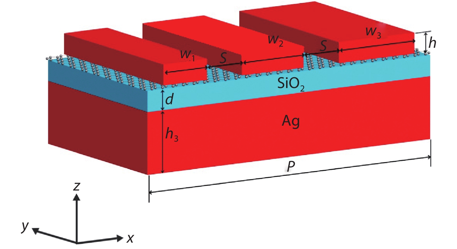
Fig. 1 shows the representation of the proposed hybrid nanostructure, which consists of silver (Ag) metal grating, monolayer graphene layer, silica (SiO2) layer and Ag substrate from top to bottom. In the unit cell of the hybrid nanostructure, w1, w2 and w3 are three gratings widths, respectively, s is grating spacing, h is the thickness of grating, d is the thickness of SiO2 spacer, hs is the thickness of Ag substrate and P is the period of unit cell.
![]()
Figure 1.(Color online) The proposed hybrid nanostructure to broaden graphene absorption bandwidth.
In numerical calculations, the computational model is three-dimensional (3D), and the length in the y direction is 3 μm. The refractive index of SiO2 is set to be 1.45, and the relative dielectric constant of Ag is expressed by drude model[
Under the random-phase approximation, the complex frequency-dependent surface conductivity σ can be expressed as the sum of the intraband σintra and interband conductivity σinter[
where e is electron charge, ħ is reduced Planck’s constant, μc is chemical potential, Γ = 1/2τ is phenomenological scattering rate[
where ε0 is vacuum dielectric constant, tg is the thickness of monolayer graphene layer. In our calculations, T = 300 K, μc = 0.1 eV, tg = 0.5 nm.
3. Results and analysis
Fig. 2 shows the calculated absorption spectra of monolayer graphene at normal incidence, under single-width and triple-widths conditions. These results are calculated by FDTD (finite-difference time-domain) simulation, FDTD can directly simulate the distribution of field and has high accuracy, and it is one of the most widely used numerical simulation methods at present. In single-width case, black, red and blue lines represent absorption efficiencies of graphene at grating width 0.14, 0.16, and 0.18 μm respectively. It can be clearly seen from Fig. 2 that for such single-width gratings, absorption bandwidth is very narrow, the bandwidth only 0.086 μm. The three absorption peaks are caused by magnetic dipole resonances.
![]()
Figure 2.(Color online) The absorption spectra of monolayer graphene in the wavelength range from 0.8 to 1.8
If we put these three different gratings stripe in a period, forming a triple-widths grating, the graphene absorption bandwidth with absorption efficiency over 30% can reach 0.311 μm, as denoted by the gray line in Fig. 2. The broadening of graphene absorption bandwidth is due to the spectrally overlapping of magnetic dipole resonances caused by the three different gratings. However, it should be noticed that absorption peaks of triple-widths grating is slightly shifted from single-width gratings.
By calculating Maxwell's equations and combining with boundary conditions, the magnetic field distribution at resonance wavelength is obtained. The magnetic field distribution of the hybrid nanostructure at resonance wavelength of λ11, λ22, λ33 are shown in Fig. 3, which are related to magnetic dipole resonances. At resonance wavelength λ33, the magnetic fields are mainly confined to the SiO2 spacer under the third Ag grating with a width w3 (see Fig. 3(c)), whereas at the resonance wavelength λ11, the magnetic fields are not only highly limited to SiO2 spacer under the first Ag grating with a width w1, but also some magnetic fields are confined to the SiO2 spacer under the second Ag grating with a width w2 (see Fig. 3(a))[
![]()
Figure 3.(Color online) Distribution of magnetic field at different resonance wavelengths on the
Fig. 4 shows effect of grating width on absorption peaks. From Fig. 4(a) to Fig. 4(c), the width w1, w2 and w3 of Ag gratings are increased gradually. It can be seen from Fig. 4 that when the widths of gratings are decreased, the absorption peaks will be blue-shifted. This phenomena can be explained by formula[
![]()
Figure 4.(Color online) Effect of grating width on absorption peaks. Structure parameters:
where c0 is the speed of light in free space, λMP is magnetic dipole resonance wavelength, C is the capacitance, which is introduced by the Ag grating and Ag substrate, the capacitance is determined by SiO2 spacer thickness, contact area between grating and substrate , electronic distribution on metal surface. Lm and Le are mutual inductance and self-inductance, which are also introduced by the Ag grating and Ag substrate[
Not only widths of gratings can affect graphene absorption peaks, but also the SiO2 spacer thickness, as shown in Fig. 5. In Fig. 5 we can clearly see as the SiO2 spacer thickness increases, the graphene absorption peaks will be blue-shifted, the phenomenon can also be explained by Eq. (5): when the SiO2 spacer thickness increases, the spacing between Ag gratings and Ag substrate will get larger, which leads to capacitance C gets smaller, therefore λMP will be blue shifted.
![]()
Figure 5.(Color online) Effect of SiO2 spacer thickness on absorption peaks. Structure parameters:
We then investigate the influence of grating spacing s on graphene absorption peaks. From Fig. 6 we can find that the grating spacing almost has no effect on the graphene absorption peaks, owing to the fact that most of magnetic fields are almost confined to the SiO2 spacer directly under the Ag gratings, only small magnetic fields is concentrated near the left and right edges of the Ag gratings (see Fig. 2).
![]()
Figure 6.(Color online) Effect of grating spacing on absorption peaks. Structure parameters:
4. Conclusion and perspective
In summary, a hybrid nanostructure consisting of a monolayer graphene sandwiched between three Ag gratings with different widths and a SiO2 spacer on an Ag substrate is proposed to broaden monolayer graphene absorption bandwidth. The wide absorption bandwidth is related to the magnetic dipole resonances, which are excited between the three different widths Ag grating and Ag substrate. Absorption bandwidth of 0.311 μm in near-infrared region is demonstrated with the absorption efficiency over 30% and the dependence of absorption peaks on Ag grating widths and SiO2 spacer thickness is also studied.
References
[1] B Zhao, J M Zhao, Z M Zhang. Enhancement of near-infrared absorption in graphene with metal gratings. Appl Phys Lett, 105, 031905(2014).
[2] R R Nair, P Blake, A N Grigorenko et al. Fine structure constant defines visual transparency of graphene. Science, 320, 1308(2008).
[3] C Lee, X Wei, J W Kysar et al. Measurement of the elastic properties and intrinsic strength of monolayer graphene. Science, 321, 385(2008).
[4] F Xia, H Yan, P Avouris. The interaction of light and graphene: basics, devices, and applications. Proce IEEE, 101, 1717(2013).
[5] M Furchi, A Urich, A Pospischil et al. Microcavity-integrated graphene photodetector. Nano Lett, 12, 2773(2012).
[6] H Lu, B P Cumming, M Gu. Highly efficient plasmonic enhancement of graphene absorption at telecommunication wavelengths. Opt Lett, 40, 3647(2015).
[7] W Zhao, K Shi, Z Lu. Greatly enhanced ultrabroadband light absorption by monolayer graphene. Opt Lett, 38, 4342(2013).
[8] D Xu, X Yu, L Yang et al. Design and photovoltaic properties of graphene/silicon solar cell. J Electron Mater, 47, 1(2018).
[9] H Xu, X Han, X Dai et al. High detectivity and transparent few-layer MoS2/glassy-graphene heterostructure photodetectors. Adv Maters, 30, e1706561(2018).
[10] J T Liu, N H Liu, J Li et al. Enhanced absorption of graphene with one-dimensional photonic crystal. Appl Phys Lett, 101, 666(2012).
[11] B Zhao, J M Zhao, Z M Zhang. Resonance enhanced absorption in a graphene monolayer using deep metal gratings. J Opt Soc Am B, 32, 1176(2015).
[12] S A Nulli, M S Ukhtary, R Saito. Significant enhancement of light absorption in undoped graphene using dielectric multilayer system. Appl Phys Lett, 112, 073101(2018).
[13] Y Cai, J Zhu, Q H Liu. Tunable enhanced optical absorption of graphene using plasmonic perfect absorbers. Appl Phys Lett, 106, 043105(2015).
[14] B Liu, C Tang, J Chen et al. Multiband and broadband absorption enhancement of monolayer graphene at optical frequencies from multiple magnetic dipole resonances in metamaterials. Nanoscale Res Lett, 13, 153(2018).
[15] G Pirruccio, M L Martín, G Lozano et al. Coherent and broadband enhanced optical absorption in graphene. Acs Nano, 7, 4810(2013).
[16] X Shi, L Ge, X Wen et al. Broadband light absorption in graphene ribbons by canceling strong coupling at subwavelength scale. Opt Express, 24, 26357(2016).
[17] F Gao, Z Zhu, W Xu et al. Broadband wave absorption in single-layered and nonstructured graphene based on far-field interaction effect. Opt Express, 25, 9579(2017).
[18] S Agarwal, Y K Prajapati. Broadband and polarization-insensitive helix metamaterial absorber using graphene for terahertz region. Appl Phys A, 122, 561(2016).
[19] H Chen, X X Zhang, H Wang et al. Near-infrared absorption of graphene-metal nanostructure based on magnetic polaritons. Acta Physica Sinica, 67, 118101(2018).
[20] J Gao, T Sang, J L Li et al. Double-channel absorption enhancement of graphene using narrow groove metal grating. Acta Physica Sinica, 67, 184210(2018).
[21] B Liu, C J Tang, J Chen et al. Dual-band light absorption enhancement of monolayer graphene from surface plasmon polaritons and magnetic dipole resonances in metamaterials. Opt Express, 25, 12061(2017).
[22] T Sang, R Wang, J Li et al. Approaching total absorption of graphene strips using a c-Si subwavelength periodic membrane. Opt Commun, 413, 255(2018).
[23] Z Zhao, G Li, F Yu et al. Sub-wavelength grating enhanced ultra-narrow graphene perfect absorber. Plasmonics, 13, 1(2018).
[24] X He, W Shi, Z Y Zhao. Graphene-supported tunable near-IR metamaterials. Opt Lett, 40, 178(2015).
[25] L Zhang, L Tang, W Wei et al. Enhanced near-infrared absorption in graphene with multilayer metal-dielectric-metal nanostructure. Opt Express, 24, 20002(2016).


Set citation alerts for the article
Please enter your email address

© Copyright 2018-2021 | Chinese Laser Press. All Rights Reserved 沪ICP备15018463号-20