1Department of Applied Physics, Beihang University, Beijing 100191, China
2State Key Laboratory of Luminescence and Application, Changchun Institute of Optics, Fine Mechanics and Physics, Chinese Academy of Sciences, Changchun 130033, China
Ming Zheng, Qingnan Yu, Hanxu Tai, Jianwei Zhang, Yongqiang Ning, Jian Wu. Experimental investigation of spontaneous emission characteristics of InGaAs-based indium-rich cluster-induced special quantum structure[J]. Chinese Optics Letters, 2020, 18(5): 051403
Copy Citation Text
The unamplified spontaneous emission (SE) is one of the important physical processes of the light–matter interaction in a diode laser in terms of Einstein’s theory. The recent research on a kind of new indium-rich cluster (IRC) laser structure did not reveal SE characteristics of the IRC structure, as its unusual quantum confined structure made it difficult to acquire correctly the SE spectra through theoretical simulation or previous experimental techniques. Thus, in this Letter, we firstly established a convenient and effective experimental approach to acquire SE spectra of the IRC structure by the measurement of amplified SEs from dual facets of a single edge-emitting chip with little sample processing. With the proposed method, the special SE spectra due to the IRC effect were observed. Then, the SE formation mechanism and characteristics in the IRC structure were analyzed by comparing the experimental data with theoretical SE spectra using a standard InGaAs/GaAs quantum well with similar material composition. This research provides a useful tool to investigate the SE characteristics of any non-standard diode laser structure and is very meaningful to develop a new type of IRC lasers.
The unamplified spontaneous emission (SE) intensity is an important parameter to consider in the design and investigation of semiconductor lasers, as it describes a fundamental physical process in light–matter interaction in terms of Einstein’s theory[1–6]. In general, the SE of a classic or standard diode laser structure can be characterized by theoretical simulation[7]. However, the theoretical calculation cannot fully reveal the SE characteristics of a non-standard quantum confined structure due to the existence of any defects in a true material system. Therefore, some experimental methods were developed in the past. These approaches involved the direct SE measurement by opening a top-contact window from the sample[8], the measurement of amplified SE (ASE) spectra by fabricating a special multi-section edge-emitting sample[9], or the measurement of the rays traveling nearly parallel to the top surface by utilizing a buried hetero-structure[10]. A common point of these methods is that additional and strict sample processing is required. This limits their application in many cases, as it is difficult to prepare such a sample. Therefore, a simpler and effective experimental approach to obtaining the SE spectra of any diode laser structure is expected firstly.
The recent research on a kind of new indium-rich cluster (IRC) laser structure has shown that the IRC effect would give rise to an irregular quantum confined structure in the InGaAs-based material system[11,12], where the IRCs were commonly regarded as a kind of defect to avoid for a standard InGaAs quantum well in the past. This means that it is difficult to characterize correctly the SE characteristics of the IRC structure through purely theoretical simulation, and it is necessary to develop a simpler and effective experimental approach to solve the SE characterization problem for the IRC quantum confined laser structure.
Based on the above statement, here, we firstly fabricated the IRC laser samples and developed a simpler and effective experimental approach to acquire the SE spectra for the InGaAs-based IRC laser structure. The method used only a single edge-emitting chip without any complicated sample processing except coating by complete transmittance at one facet of the chip. This avoided unnecessary measurement errors from inaccurate sample processing. Subsequently, the experimental SE data of the IRC structure were analyzed by comparing the theoretical SE spectra using a standard InGaAs/GaAs quantum well with similar material composition. Finally, the conclusions were stated.
Sign up for Chinese Optics Letters TOC. Get the latest issue of Chinese Optics Letters delivered right to you!Sign up now
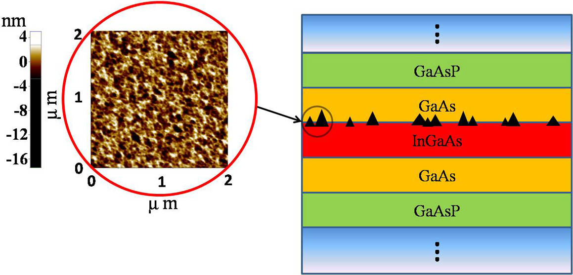
The IRC laser sample was designed with as the original active layer material, the thickness of which was 10 nm. A 2-nm-thick GaAs strain-compensating layer was embedded between the active layer and a barrier to relieve the high compressive strain between the active layer and the barrier. The waveguide was the AlGaAs material with a thickness of 2 μm. The whole structure is grown on the GaAs (001) substrate with metal organic chemical vapor deposition. The temperature for the material deposition was 660°C. The higher temperature of 660°C was applied here to increase the migration length of the indium atoms in the material growth process. This would be beneficial to the IRC’s formation[13–16]. The material growth rate was 0.2 nm/s under 100 mbar pressure.
The laser structure is shown in Fig. 1, where the left image within a red circle shows the IRCs and their distribution on the surface of the InGaAs active layer. These IRCs were observed and recorded using an atomic force microscope (AFM) (Park Systems Instrument Co., Ltd., model XE100). From the AFM picture, it can be measured that the IRC sizes are about .
Figure 1.Diagram of the InGaAs-based IRC structure. The left image shows the IRCs on the InGaAs surface, which were recorded with an AFM.
In general, the IRCs are comprised of indium atoms or InAs compounds. These clusters have various sizes and irregular distribution and lead to the indium content being lost from the InGaAs material. Thus, the original InGaAs active layer is fragmented into many smaller InGaAs active regions with various areas and different indium contents, which will produce the SEs in the spectral range of .
The experimental principle to obtain the SE spectra of the IRC laser structure is described below. An edge-emitting sample is coated by the complete transmittance () at one end and uncoated at the other end, the reflectivity () of which is determined by the index of the active layer[17]. A beam of a pulsed and intensity-uniform 808 nm laser is used to shine the top surface of the sample as optical injection. The ASE intensities of and are measured at both ends of the sample, respectively, using a spectrometer, as shown in Fig. 2. The ASE intensities can be expressed as[18]where denotes the SE intensity, is the sample length, and denotes the modal gain of the device. By combining Eqs. (1) and (2) to remove the gain coefficient, the SE intensity is expressed as
Figure 2.Principle of measuring ASE spectra from both ends of the sample under optical injection to obtain the SE spectra of the IRC laser structure.
The sample for the experiment was in area, which was coated by the transmittance of at one facet and uncoated at the other one, the reflectivity of which is evaluated as . The ASE spectra from both ends were obtained with an injection carrier density of . The results are shown in Fig. 3. Therefore, the SE spectra are obtained by substituting the ASE data into Eq. (3). The results are shown in Fig. 4.
Figure 3.ASE spectra of TE and TM polarization modes, which were measured from both ends of the edge-emitting IRC laser sample with an injection carrier density of .
The result in Fig. 4 shows two unusual features different from the SE spectra of a standard InGaAs/GaAs quantum well. One is that the SE spectral range is increased up to for both TE and TM modes. The other is that double peaks emerge in the SE spectra for both TE and TM polarization modes. The increased SE bandwidth can be interpreted by the combination of different SEs produced by the multiple fragmented InGaAs active regions due to the IRC effect. As these regions have different areas and indium contents, the band-gaps formed within them will be a little different from each other. Therefore, the SE spectra from these regions will have peak offsets from each other in the SE superposition.
The double-peak appearances in both TE and TM SE spectra are explained here by the model-solid theory[19]. The analysis on the InGaAs band-gaps and photon energies shows that the double peaks in Fig. 4(a) are exactly in correspondence with the emissions of the materials with and , respectively. This means that the fragmented regions in the active layer can be divided principally into two categories, according to the indium content, i.e., and for the given sample. These regions lead to a special band structure with hybrid strains, as shown in Fig. 5, which is formed by joint actions of the compressive strain in the part and the tensile strain in the part due to lattice mismatching. Thus, the different band-gaps are generated in the whole active medium, the photon energies from which are in correspondence with the multiple peaks in the SE spectra. As a result, both peak A () in the TE SE curve and peak C () in the TM SE curve in Figs. 4(a) and 4(b) are principally formed due to the electron-hole recombination in the compressively strained regions. The peak A is higher than peak C because of its emission corresponding to the smallest band-gap, as shown in Fig. 5. Meanwhile, both peak B () in the TE SE curve and peak D () in the TM SE curve in Figs. 4(a) and 4(b) are principally formed from the electron-hole recombination in the tensile-strained regions. The band-gap between the first conduction sub-band () and the first valence sub-band of light-holes () is shown in Fig. 5 as well.
Figure 5.Hybrid band structure consisting of the first conduction sub-band () and the first valence sub-bands of heavy holes (, black line) and light holes (, blue line) due to the IRC effect in the material system.
In the regions, and sub-bands generate the offsets of and , respectively, due to the compressive strain. Thus, there is an energy difference of between the and sub-bands in the valence band, which corresponds to the energy difference between peaks A and C in the SE spectra. Also, there is an energy difference of between the and sub-bands in the regions, which corresponds to the energy difference between peaks B and D in the SE spectra, where the and sub-bands generate the offsets of and , respectively, due to tensile strain[20]. The mixed band structure due to the existence of both tensile and compressive strains in the IRC structure makes it possible to simultaneously generate polarization-independent TM and TE emissions, according to Fig. 5 and Ref. [21].
In order to analyze further the experimental results, the purely theoretical calculation on the SE intensity with an ideal or standard quantum well without the IRC effect is carried out by the following equations[9]: where is the inversion factor depending solely on the occupation probabilities for the initial and final states of the transition. Thus, the SE intensity can be theoretically expressed as follows by combining Eqs. (4) and (5): where is the inversion factor. is the constant related to the sample. represents the Fermi-level separation of the conduction band and the valence band, which can be evaluated from the optical gain[22]. is the temperature, and is the gain as a function of photon energy. is the Boltzmann constant, and is Planck’s constant. and are the scaling factor and the optical confinement factor of the laser structure, respectively. is the light speed in vacuum, and is the refractive index of the material[23]. The results are shown in Fig. 6.
Figure 6.Theoretical SE spectra in (a) TE mode and (b) TM mode with different injection carrier densities, where solid lines are the calculated SE curves with a standard quantum well regardless of the IRC effect, and dash lines are the experimental data from the InGaAs IRC laser sample.
Figure 6 shows two distinct points. One is that the experimental SE spectra (dash lines) from the InGaAs IRC structure are basically consistent with the theoretical SE curves (solid lines) of a standard InGaAs quantum well regardless of the IRC effect in the long wavelength direction around peak A in Fig. 6(a) and in the short wavelength direction around peak C in Fig. 6(b). This is because the original regions take a dominate role in the SE generation for both TE and TM modes. The slight difference between them is because of the additional contribution from the regions formed due to the IRC effect on the experimental SE spectra. The other is that there are big differences between the theoretical and experimental SE spectra in the short wavelength direction around peak B in Fig. 6(a) and in the long wavelength direction around peak D in Fig. 6(b). This is because the IRC-induced regions take a dominate role in the SE generation for both TE and TM modes.
In summary, the special SE characteristics of a kind of new InGaAs-based IRC quantum confined laser structure were experimentally investigated for the first time, to the best of our knowledge. The SE spectra were acquired by measuring the ASE intensities at the two ends of a single edge-emitting IRC laser chip with little sample processing. The special double-peak phenomenon in the SE spectra due to the IRC effect was observed. The explanation of it was based on the analysis of the SE superposition from the fragmented InGaAs regions, which have different areas and indium contents, as well as the hybrid band structure formed in the InGaAs/GaAs IRC structure. The theoretical SE intensities of an ideal or standard InGaAs/GaAs quantum well were calculated and compared with the experimental SE spectra from the InGaAs/GaAs IRC structure. This work provides a useful tool to investigate the SE characteristics of any non-standard diode laser structure and is very meaningful to investigate and develop a new type of IRC diode laser with some unusual functions.