• Journal of Semiconductors
  • Vol. 41, Issue 11, 112401 (2020)
Xiangxin Pan, Xiong Zhou, Sheng Chang, Zhaoming Ding, and Qiang Li
Author Affiliations
  • Institute of Integrated Circuits and Systems, University of Electronic Science and Technology of China, Chengdu 610054, China
  • show less
    DOI: 10.1088/1674-4926/41/11/112401 Cite this Article
    Xiangxin Pan, Xiong Zhou, Sheng Chang, Zhaoming Ding, Qiang Li. A 12-bit 30-MS/s VCO-based SAR ADC with NOC-assisted multiple adaptive bypass windows[J]. Journal of Semiconductors, 2020, 41(11): 112401 Copy Citation Text show less

    Abstract

    This paper proposes a technique that uses the number of oscillation cycles (NOC) of a VCO-based comparator to set multiple adaptive bypass windows in a 12-bit successive approximation register (SAR) analog-to-digital converter (ADC). The analysis of the number of bit cycles, power and static performance shows that three adaptive bypass windows reduce power consumption, and decrease DNL and have similar INL, compared with the SAR ADC without bypass windows. In addition, a 1-bit split-and-recombination redundancy technique and a general bypass logic digital error correction method are proposed to address the settling issues and optimize the size of the bypass window. This design is implemented in 40 nm CMOS technology. The conversion frequency of the ADC reaches up to 30 MS/s. The ADC achieves an SFDR of 85.35 dB and 11.12-bit ENOB with Nyquist input, consuming 380 μW, down from 427 μW without multiple adaptive bypass windows, at a 1.1 V supply, resulting in a figure of merit (FoM) of 5.69 fJ/conversion-step.

    1. Introduction

    Low power and high resolution analog-to-digital converters (ADCs) are widely used in mobile, wearable and implantable devices, the internet of things (IoT) and so on. Successive approximation register (SAR) ADC exhibits excellent energy efficiency and has attracted much attention due to its digital-like nature and adaptability to advanced CMOS technology. Much work is occuring to reduce the logic power consumption, such as a variety of switching schemes to save part of the energy of CDAC[1-6]. From a systematic perspective, the bypass logic shown in Fig. 1, can not only save energy from CDAC but also greatly reduce the energy from the comparator and digital logic[7]. When the input voltage is within the range called the bypass window, the intermediate bit cycles can be skipped completely and does not influence the correct output. However, the bypass window comes at the cost of two additional coarse comparators and an external reference, which increases design complexity and makes the precision partially dependent on the reference voltage.

    Conversion process of 6-bit SAR ADC. (a) Conventional SAR ADC. (b) SAR ADC with bypass window.

    Figure 1.Conversion process of 6-bit SAR ADC. (a) Conventional SAR ADC. (b) SAR ADC with bypass window.

    The comparator is a fundamental consideration in SAR ADC, which is an indispensable but power-hungry block. The input-referred noise constrains the power consumed by the comparator. For a voltage-domain comparator such as a double-tail comparator or strong-arm comparator, whose noise reduction relies on brute-force analog scaling, it requires four times the power to halve the input-referred noise[8]. Alternatively, time-domain comparators, which show good potential in power efficiency and scalability, attract attention due to their digital nature and more choices for lower noise such as VTC-based[9], VCDL-based[10], oscillator collapse-based[11] and VCO-based[12, 13]. The last type gains much favor under its noise-adaptive characteristic. It can generate output signal without oscillation if the input voltage is large. When the input voltage is small enough, it will oscillate until the decision is made. In other words, there is a relationship between the input voltage and the oscillation number, which shows that the oscillation number indicates an inherent coarse quantization.

    Apart from making decisions and employing the decisions to reduce the comparator noise[14-16], a VCO-based comparator offers extra information, known as the number of oscillation cycles (NOC)[17], to detect whether the input signal of the comparator is in the vicinity of common-mode voltage. This information can be utilized to trigger bypass logic, which avoids the use of additional comparators and reference. It can be triggered at any bit as long as NOC reaches a specific number. Furthermore, multiple bypass windows can be constructed by NOC, which provide more power reduction and static performance improvement. The windows size can be adaptively adjusted to PVT variations on the basis of the NOC and window detection logic.

    This design takes full advantage of the potential of a VCO-based comparator as a bypass detector served, which can be used for higher resolution (12 bit) and higher speed (30 MS/s) SAR ADC[18]. The structure of the VCO-based comparator and the consideration of the offset caused by different NOC are presented. The design of core digital circuits is described thoroughly. The benefits of bit cycles decrease, power reduction and static linearity improvement from adaptive multiple bypass windows are analyzed. For compensating the settling error from DAC and reference because of high resolution and speed, a 1-bit split-and-recombination redundancy[19] and a general method to correct digital errors for bypass logic are proposed, which circumvents the use of complex or off-chip calibration circuits.

    This paper is organized as follows. Section 2 describes the overall ADC architecture, operation principle and building blocks. Section 3 analyzes the bit cycle decrease, power reduction and static performances with multiple adaptive bypass windows, and derives the maximum DNL and INL of it, while section 4 explains split-and-recombination based redundancy and a general digital error correction method for bypass logic. Section 5 presents simulation results and comparison with the state-of-the-arts, and section 6 draws the conclusions.

    2. Architecture and design considerations

    The architecture of the proposed SAR ADC is shown in Fig. 2 including two bootstrapped sampling switches[20], a differential capacitive DAC (with 1-bit redundancy), VCO-based comparator, NOC counter, SAR logic, bypass logic, window detection logic (three adaptive bypass windows), window update logic, and digital error correction logic.

    Architecture of the proposed SAR ADC.

    Figure 2.Architecture of the proposed SAR ADC.

    2.1. Operation principle

    During the sampling phase, the input differential voltage is sampled onto the top plates of CDAC by two bootstrapped switches. If the input signal is large enough, the comparator makes the decision directly without oscillation. Otherwise, if the input signal is relatively small (within several LSBs), VCO will oscillate several times to increase the delay until the time difference between two VCO loops exceeds the dead zone of the phase detector. To take advantage of the oscillation information, three bypass windows W2, W3 and W4 are used for the standing of the oscillation numbers of 2, 3 and 4, respectively. For example, if the NOC is 4, the bypass window W4 is triggered for the first time and bit cycles will move to the LSB cycle. Due to the impact of noise and PVT variation, even if the same voltage inputs into the comparator, the oscillation number might be different. The signal must be detected to determine whether it can be digitized with the remaining capacitor weights in case the result is not convergent.

    Window update logic, shown in Fig. 3, can implement the window-size detection. and are the differential inputs. stands for the current bypass window size of W4, and its initial value is 1 LSB. If differential signals cannot cross zero (common-mode voltage), the bypass window is too small and this process of the bypass is wrong[17]. The cycle must be back to where the bypass begins and W4 is updated. The next time when the NOC is 4, the conversion process will be bypassed to the cycle of LSB + 1 and will become the voltage of 2 LSB. This update process also applies to W2 and W3. It is worth noting that the size of the bypass window is updated following the weights of CDAC and carried out in the background. So smaller low-weight capacitors achieves more precision bypass window sizes and the adaptive bypass windows are PVT-robust. Bypass logic cannot be triggered for more than one time in one conversion period under the consideration of conversion speed and complexity of the logic design.

    Window update logic. (a) Not cross zero. (b) Cross zero.

    Figure 3.Window update logic. (a) Not cross zero. (b) Cross zero.

    2.2. VCO-based comparator design and offset consideration

    Compared with voltage-domain comparator, whose input-referred noise is often dominated by sizes of input and tail transistors[21], designing a low-noise VCO-based comparator is more flexible[17]. The more stages it uses, the lower input referred noise but lower speed for the large input voltage it possesses. For delay cells, the topologies, the sizes of transistors, the threshold voltages of transistors and filtering capacitors all influence the noise and speed[22]. It is a hard trade-off that influences the bypass window sizes. Two common different delay cells are shown in Fig. 4. When input voltage is low, the pulling down of cell II will be slow. Compared with the delay cell II[12], the inserted inverter in delay cell I increases the reset speed. The option is that four stages of the delay cell I are to be used in the proposed scheme for quicker comparison.

    Schematic of two common delay cells.

    Figure 4.Schematic of two common delay cells.

    Some works[23, 24] utilized multiple comparators to achieve lower power consumption or higher speed[25, 26]. All these designs have the matching problem of different input-referred offset voltages, which can be solved well by the calibration method[27] or introducing redundant capacitors into the DAC[28]. Actually, a VCO-based comparator operates like multiple comparators as it oscillates for a different number of cycles while it does not need extra calibration circuit or redundant cycle. The offset problem must be analyzed very carefully.

    The delay time of the unit delay stage is given by

    $ t_{\rm{d}} = \frac{{C_{\rm{L}}} V_{\rm{dd}}}{2I_{\rm{DS}}}, $ (1)

    where and are the load capacitance and average current of the current-starving stage, respectively. And the differential voltage-to-time gain of the VCO for one oscillation cycle is given by

    $ G_{{\rm{VCO}}\_1} = \frac{2C_{\rm{L}} V_{\rm{dif}} g_{\rm{m}}}{I_{\rm{DS}}^{2}} , $ (2)

    where is the trans-conductance of the tail NMOS, and is the differential input voltage of the VCO comparator.

    The dead zone of the PD ( ) represents the minimum detectable delay difference. The difference input voltage has the following relationship with the number of oscillations [17],

    $ \left | (n-1)G_{{\rm{VCO}}\_1} V_{\rm{dif}} \right |\leqslant t_{\rm{dz}}< \left | nG_{{\rm{VCO}}\_1} V_{\rm{dif}} \right | . $ (3)

    According to Eq. (2), Eq. (3) can be rewritten as

    $ \frac{t_{\rm{dz}}I_{\rm{DS}}^{2}}{2ng_{\rm{m}}C_{\rm{L}}V_{\rm{DD}}}< \left | V_{\rm{dif}} \right |\leqslant \frac{t_{\rm{dz}}I_{\rm{DS}}^{2}}{2(n-1)g_{\rm{m}}C_{\rm{L}}V_{\rm{DD}}} . $ (4)

    Eq. (4) means that the number of oscillaitons is the coarse quantization of the input signal, i.e., each NOC value corresponds to an input range.

    Since the current of the unbiased circuit is much larger than that of the biased transistor, the offset voltage caused by the unbiased circuit can be ignored. For one oscillation cycle, the VCO in Fig. 5 can be considered as a four-stage VCDL. Hence, according to Ref. [10], the standard deviation of the offset time due to one oscillation cycle can be written as

    Schematic of VCO-based comparator and phase detector.

    Figure 5.Schematic of VCO-based comparator and phase detector.

    $ \Delta t_{{\rm{dVCO}}\_1} = \frac{g_{\rm{m}}\Delta V_{\rm{os}}C_{\rm{L}}V_{\rm{dd}}}{I_{\rm{DS}}^{2}} , $ (5)

    where is the standard deviation of the input-referred offset voltage of one delay stage. And the standard deviation of the input-referred offset voltage induced by single oscillation becomes

    $ \Delta V_{{\rm{osVCO}}\_1} = \frac{\Delta t_{{\rm{dVCO}}\_1}}{G_{{\rm{VCO}}\_1}} = \frac{\Delta V_{\rm{os}}}{2}. $ (6)

    No matter how many cycles are needed in the oscillation loop, signals oscillate in the same circuit paths. The offset delay time of a fabricated chip remains unchanged for each oscillation cycle. Hence, the standard deviation of the offset time caused by n oscillation cycles is . So the input-referred offset voltage for n oscillation cycles is

    $ \Delta V_{{{\rm{osVCO}}}\_n} = \frac{n\cdot \Delta t_{{\rm{dVCO}}\_1}}{G_{{{\rm{VCO}}}\_n}} = \frac{\Delta V_{\rm{os}}}{2}. $ (7)

    Eqs. (6) and (7) show that the input-referred offset voltage of the VCO-based comparator for one oscillation cycle is the same as that of n oscillation cycles.

    The NAND-based phase detector (PD) is shown in Fig. 5. Compared with the DFF-based PD in Ref. [12], it needn't wait for a slower edge. Therefore, it increases the speed of the comparator. The size of the dead zone and bypass window can be tuned via load capacitors.

    The dead zone of the PD can be derived as

    $ t_{\rm{dz}} = \frac{(C_{3}-C_{2})V_{\rm{dd}}}{2I_{\rm{NAND}}} , $ (8)

    where and are the load capacitors at the output terminals in PD, is the supply voltage and is the average switching current of NAND. The simulated results of the dead zone of PD are shown in Fig. 6, which is accorded with Eq. (8).

    Comparison of simulated result and Eq. (6) of the dead zone of PD.

    Figure 6.Comparison of simulated result and Eq. (6) of the dead zone of PD.

    2.3. Capacitive DAC

    This work employs a split capacitor switching scheme[29] from MSB to LSB + 1. Compared with many other switching schemes, it not only keeps the input common-mode voltage of comparator stable, which avoids the deterioration of linearity of ADC, but also eliminates the need of extra common-mode voltage. For the LSB, the design uses the monotonic switching procedure[30]. It can halve the total capacitance with a fixed unit capacitor. Moreover, the change of common-mode voltage caused by it is negligible. To meet the requirements of KT/C noise and matching, this design chooses the unit capacitor as 1fF. The weight of the capacitor is shown in Fig. 1.

    2.4. Bit-cycle control logic

    In this design, the order of bit cycles is controlled by NOC. Bit cycles are not executed in the order of the conventional SAR ADC because of the bypass and window update logic. Registers should record the current cycle number, cycle number after bypass and the window size after window updating.

    Fig. 7(a) shows the schematic and timing diagram of bit cycle control logic. It employs three window registers to record the sizes of three predefined bypass windows. Because of the relatively small size of the window, a 5-bit register can implement every window. CLR is the reset signal to reset window registers at power-up. The signal consists of , , and . The rising edges of them mean that differential input voltage triggers the corresponding window. The bypass cycle register is utilized to record the bit cycle after the process of the bypass. The decision of the comparator is indicated by the signal , and is the delay signal of . The normal cycle register is used to record the current bit cycle in the normal SA process. Enabling the bypass cycle register or normal cycle register is selected by the signal SEL. And is the inverted sampling signal and is used to control the state of CDAC.

    Bit cycle control circuits. (a) Schematic. (b) Timing diagram.

    Figure 7.Bit cycle control circuits. (a) Schematic. (b) Timing diagram.

    Fig. 7(b) shows the timing diagram of the bit cycle control logic for two conversion periods. Initial CLR is low to reset the window registers. When is low, both the bypass cycle register and the normal cycle register are reset. A low means that normal cycle register is enabled. is set high when the next rises meaning that the 12th bit is being converted. If the bypass logic is not triggered, the SA cycle will convert the 11th cycle. However, the rising edge of means that the bypass window is triggered. A high enables the bypass cycle register and disables the normal cycle register. At the same time, the high makes connect to , and it is set to high. becomes high on the next rising edge, meaning that the conversion from the 11th to the 2nd bit cycle is skipped and the conversion of the 1st bit starts. The rising edge of indicates that is outside the bypass window and the window is too small. So the value of the window register increases by one. Then is set to low to disable the bypass cycle register and enable the normal cycle register. At the same time, is reconnected to . Therefore, the bit cycles previously bypassed is reconverted, and the 11th bit will be converted in the next cycle.

    At the beginning of next sampling period, SEL is low and it is a conventional SA process. The rising edge of triggers the bypass logic. Since has increased from to . Then the cycles from the 11th to the 3rd are bypassed. Missing the window size error detection during this cycle, is set to high on the next rising edge of .

    2.5. CDAC driving circuits

    In this design, the CDAC needs to be recovered after the detection of the wrong window size sometimes. The driving circuits of CDAC are shown in Fig. 8. and are delay signals of the comparator output. and are inverted signals of and , respectively. When is low, is set to high and is set to low. If is high, high can set to high and low can lock all outputs until the next effective . Similarly, if is high, high can set to high and low can lock all outputs until the next effective .

    CDAC driving circuits. (a) Blocks. (b) Schematic. (c) Timing diagram.

    Figure 8.CDAC driving circuits. (a) Blocks. (b) Schematic. (c) Timing diagram.

    In the upper block in Fig. 8(a), can be used as a reset signal to reset this block in the sampling phase. can work as the reset signal in the lower block to recover the wrong switches due to the wrong bypass window size. For example, in Fig. 7, in the first sampling period, after the rising edge of , the output of the comparator is locked in and . At this moment, the window size is wrong. So the rising edge of set to low, so and are reset directly. Therefore, these circuits do not need extra blocks to complete the recovery from the wrong switches in CDAC.

    3. Multiple adaptive bypass windows

    The NOC of the VCO-based comparator can be used to construct multiple bypass windows without additional references and comparators. The power reduction and static performances with multiple bypass windows are discussed in detail.

    3.1. Power reduction with multiple adaptive bypass windows

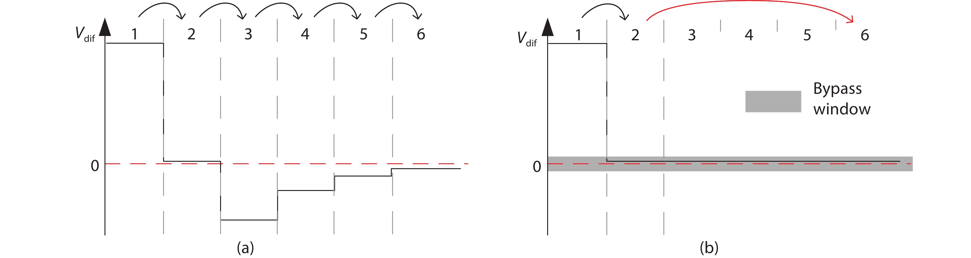
    Fig. 9 shows two conversion periods of a 6-bit SAR ADC without and with different bypass windows, respectively. In Fig. 9(a), 6 SA cycles are needed in every conversion period for conventional SAR ADC no matter how much the input signal is. For the SAR ADC with a wide bypass window, shown in Fig. 9(b), the differential signal is likely located in the range of the bypass window. But the bypass logic can only bypass a few SA cycles, and hence the power efficiency improvement is limited. For the SAR ADC with a narrow bypass window, shown in Fig. 9(c), has fewer opportunities to be detected within the bypass window. However, the bypass logic can bypass more numbers of SA cycles for the detected signal. The conversion process in Fig. 9(d) shows that the SAR ADC with multiple adaptive bypass windows will improve conversion efficiency extremely.

    Conversion processes of 6-b SAR ADCs. (a) Without bypass window. (b) Wide bypass window. (c) Narrow bypass window. (d) Multiple adaptive bypass windows.

    Figure 9.Conversion processes of 6-b SAR ADCs. (a) Without bypass window. (b) Wide bypass window. (c) Narrow bypass window. (d) Multiple adaptive bypass windows.

    For general signals with uniform input, Fig. 10 shows the number of SA cycles per sample of a 12-bit SAR ADC with different bypass windows. The voltage range of a single wide or narrow bypass windows is LSB or LSB, respectively. For the wide bypass window, the bypass logic can reduce the number of SA cycles within a large input signal range, which achieves 11.06 SA cycles per sample on average. For the narrow bypass window, though the bypass logic can be employed to deal with the smaller input signal range, it can reduce more SA cycles for the signal meeting the size of the bypass window (indicated by the red line in Fig. 10), leading to 11.69 SA cycles per sample on average.

    (Color online) SA cycles per sample. (a) Wide bypass window. (b) Narrow bypass window. (c) Multiple adaptive bypass windows.

    Figure 10.(Color online) SA cycles per sample. (a) Wide bypass window. (b) Narrow bypass window. (c) Multiple adaptive bypass windows.

    For the SAR ADC with multiple adaptive bypass windows, this design uses three bypass windows. The simulation result shows that the SAR ADC with multiple adaptive bypass windows responds to large input signal range. Additionally, for small input voltage, the bypass logic can save more SA cycles. In other words, the SAR ADC with multiple adaptive bypass windows takes advantage of both the wide and narrow bypass windows. The size of the three bypass windows is initialized to 1 LSB, when the circuit starts to work. The window size has a correction process, and the three windows corresponding to NOC = 2, 3 and 4 will eventually stabilize on a certain size[17]. The convergence results are related to the design of the VCO comparator. In this design, the sizes of the three windows converge to LSB, LSB and LSB. And the SAR ADC with three bypass windows achieves 10.75 cycles per sample on average. The power consumption of the SAR ADC mainly consists of the power of DAC, comparator and control logic. Reducing the SA cycle can reduce the power of the DAC, comparator and control logic at the same time. There is a case worth mentioning: where the clock cycles should be beyond 12 when the size of bypass window is wrong. However, because the change of window size is mainly caused by PVT change, the correct bypass window can be used in subsequent ADC conversion, without the need to detect the wrong bypass window every cycle and waste power. Consequently, the SAR ADC with multiple adaptive bypass windows can save more power than that with a single bypass window.

    When three bypass windows sizes are assumed as LSB, LSB and LSB respectively, and the probability density function of the output code is assumed as a uniform distribution, Fig. 11 shows the power consumption by switching with and without bypass logic. The average switching energy with bypass logic is 602.92 , which is 11.62% lower than the switching energy without bypass logic (682.17 ). If there is only one bypass window used, the switching energy is 605.89, 654.89 and 666.63 for , , and , respectively.

    Switching power consumption with/without bypass logic.

    Figure 11.Switching power consumption with/without bypass logic.

    It is worth noting that the narrow window like W4 failing to decrease too much bit cycles and switching power comes as no surprise. This is because the input signal is assumed as uniform here and the power efficiency of bypass logic is tied to the characteristics of signals. For many biomedical signals concentrating on the adjacent of common-mode voltage, this shows small variations in magnitude can save much power with bypass logic[7, 31]. In contrast with the single bypass window of prior works, the technique of multiple adaptive bypass windows is more versatile for different characteristics of input signals.

    3.2. Static performance analysis of SAR ADC with multiple adaptive bypass windows

    The state of capacitors in a split capacitor array is illustrated in Fig. 12. When the control code is changed from to , is switched; when the control code is changed from to , is switched. Considering the mismatch of capacitors, different error voltages are introduced into the system by and if the control codes are different.

    The state of capacitors in split capacitor array.

    Figure 12.The state of capacitors in split capacitor array.

    The output voltage of the proposed SAR ADC is given by

    $ V(S) = \frac{\sum_{i = 1}^{N-1}(C_{{\rm{up}}\_i}b_{{\rm{up}}\_i}-C_{{\rm{dn}}\_i}b_{{\rm{dn}}\_i})+C_0b_{{\rm{up}}\_0}}{C_{\rm{total}}}V_{\rm{ref}} , $ (9)

    $ \begin{array}{l} \rm{DNL} = \left[ C_{{\rm{dn}}\_N-1}-\sum\limits_{i = M+1}^{N-2}C_{{\rm{up}}\_i}-(C_{{\rm{up}}\_M}+ C_{{\rm{dn}}\_M})+\right.\\ \left.(C_{{\rm{up}}\_M-1}+C_{{\rm{cn}}\_M-1}) -\sum\limits_{i = i}^{M-2}(C_{{\rm{up}}\_i}+C_{{\rm{dn}}\_i})-C_0 \right] \cdot \dfrac{V_{\rm{ref}}}{C_{\rm{total}}}. \end{array} $ (10)

    If the control code of the DAC [ ] = 1, = 1 and = 0; if = 0, = 0 and = 1; if , = 0 and = 0. and are the actual values (with mismatch errors) of the corresponding capacitors. is the unit capacitance. Since the mismatch errors of high-weighted capacitors influence the conversion results, much more greatly than that of the low-weighted capacitors, the maximum DNL occurs at the minimum code with the largest bypass window. Assuming the maximum bypass window LSB), the maximum DNL will occurs at , which can be decoded into the standard binary code as Dout = by the state of capacitor array. The control code for Dout = is . So the voltage difference can be written as

    $ {\rm{DNL}} = V(XXXXXX010000)-V(011111101111) . $ (11)

    Assuming is the standard deviation of the random error of a unit capacitor, from Eqs. (9) and (11), the DNL can be written in LSB as . If and the resolution is N-bit, Eq. (10) can be derived. So the maximum DNL can be calculated in LSB as

    $ {\rm{DNL}}_{\rm{max}}\approx \frac{\sigma _0\sqrt{2^{N-2}+2^{M-1}}}{C_0} . $ (12)

    Fig. 13 illustrates the DNL performance of a conventional SAR ADC with split capacitor array and the proposed ADC with multiple adaptive bypass windows. The DNL curves are the root-mean-square (RMS) value of 10 000 simulations and each unit capacitor cell has a Gaussian random error with a standard deviation of 1%. The simulation shows the ADC with multiple adaptive bypass windows achieves a better DNL performance than the conventional one.

    (Color online) DNL performances of SAR ADC without bypass window and with multiple adaptive bypass windows.

    Figure 13.(Color online) DNL performances of SAR ADC without bypass window and with multiple adaptive bypass windows.

    The definition of INL at bin k is often defined as . However, in actual applications, is used as the starting point of INL to eliminate the error caused by offset. So the formula of INL is

    $ {\rm{INL}}(k) = V(k)-V(0)-V_{\rm{ideal}}(k) . $ (13)

    If the minimum bypass window LSB), the control code at Dout = is S = . The INL at Dout = is

    $ {\rm{INL}} = V(XXXXXXXXX011)-V(000000000000)-V_{\rm{ideal}} . $ (14)

    So the INL at Dout = can be calculated in LSB as . Similarly, if the minimum bypass window , the INL at Dout = is

    $ {\rm{INL}} = \left[\sum\limits_{i = K+1}^{N-1}C_{{\rm{dn}}\_i}+\sum\limits_{i = 1}^{K-1}(C_{{\rm{up}}\_i}+C_{{\rm{dn}}\_i})+C_0 \right] \frac{V_{\rm{ref}}}{C_{\rm{total}}}-V_{\rm{ideal}} . $ (15)

    Since and are different in split capacitor array because of mismatch, Eq. (14) cannot be simplified. So the maximum INL can be calculated in LSB as

    $ {\rm{INL}}_{\rm{max}}\approx \frac{\sigma _0\sqrt{2^{N-2}}}{C_0} , $ (16)

    which shows that the maximum INL is independent of the bypass window parameter K. The INL performance of the SAR ADC with multiple bypass windows (the standard deviation of the Gaussian error of the unit capacitor is 1%) is shown in Fig. 14, and it is the same with the INL performance of a conventional SAR ADC with the split capacitor array[29].

    INL performance of SAR ADC with multiple adaptive bypass windows.

    Figure 14.INL performance of SAR ADC with multiple adaptive bypass windows.

    4. Split-and-recombination-based redundancy with adaptive bypass windows

    In a high-resolution ADC with relatively high speed, variations on reference voltage lead to wrong decisions. The design avoids the large-area on-chip decoupling capacitor for stabilizing the reference by redundancy. The solution corrects the errors, and it is also favorable for the speed because the requirement for DAC settling is relaxed. Although the bypass logic offers redundancy since there are multiple output presentations for one identical input voltage[7], it is not enough for a 12-bit 30 M/s SAR ADC.

    Compared with the binary-scaled error compensation redundancy[32], the split-and-recombination redundancy[19] does not need extra compensation capacitors and the sampling capacitance and input range remains unchanged. The main idea of split-and-recombination redundancy is to split MSB into two groups and make the smaller group recombine with LSB capacitors. The most critical point is that each capacitor is not larger than the sum of capacitors smaller than it so that multiple output codes are assigned to one same input signal. A split-and-recombination method (1-bit) shown in Fig. 15 is chosen under the consideration of speed. For designing the digital error correction circuit, it is necessary to derive the expression of Dout first.

    Split-and-recombination method.

    Figure 15.Split-and-recombination method.

    4.1. Without bypass logic

    If the bypass logic is not applied, the Dout can be written as Fig. 16. And Dout also can be expressed as Fig. 17. The digital error correction logic can be designed according to this expression similar to the implementation in Ref. [19].

    Expression of Dout without bypass logic.

    Figure 16.Expression of Dout without bypass logic.

    Expression of Dout without bypass logic.

    Figure 17.Expression of Dout without bypass logic.

    4.2. With bypass logic

    The proposed bypass logic requires us to know the weights of the bypassed cycles. For example, it needs to search four times without bypass logic for as shown in Fig. 18. The weight of every bit is 8, 4, 2 and 1, respectively. So the output is obtained by . For with bypass logic, the first and second cycles are bypassed. So must be located in areas I and II. The third and fourth comparison results are 1 and 0, respectively. So the output is ( stands for the bit bypassed). In this way, the output can be expressed as .

    (Color online) Binary search with and without bypass logic.

    Figure 18.(Color online) Binary search with and without bypass logic.

    In short, bypassing one bit requires the addition of half weight of this bit to the output regardless of binary or non-binary weight. In accordance with this general conclusion for bypass logic, the Dout can be expressed as shown in Fig. 19 and red represents the nth bypassed cycle. According to the expression of Dout, digital error correction as shown in Fig. 20 rather than ROM[33] or off-chip correction can be implemented by full adders, DFFs and XORs.

    Expression of Dout with bypass logic.

    Figure 19.Expression of Dout with bypass logic.

    Part of implementation of digital error correction logic.

    Figure 20.Part of implementation of digital error correction logic.

    Adding the redundancy decreases weights of LSBs as well, e.g., the weights of and change from 16 and 8 to 10 and 6. Because the window sizes are updated along with capacitors, smaller weights of LSBs refine the step size of the update, which makes the bypass logic more power-efficient.

    5. Simulation results and comparisons

    The proposed 12-bit SAR ADC is designed in 40 nm CMOS technology. Fig. 21 shows the FFT plot of the ADC output at transistor-level simulation with a pad model. At a sampling rate of 30 MS/s, the ADC achieves an ENOB of 11.12-bit with 14.30 MHz input. The SNDR and SFDR are 68.72 and 85.35 dB, respectively. Fig. 22 shows the stable SNDR and SFDR versus different input frequency.

    (Color online) FFT plot with Nyquist input at 30 MS/s.

    Figure 21.(Color online) FFT plot with Nyquist input at 30 MS/s.

    Dynamic performance versus input frequency.

    Figure 22.Dynamic performance versus input frequency.

    The total power consumption at Nyquist frequency is 380 W. It can be broken down as shown in Fig. 23: 63% from capacitor switching and DAC buffers; 26% from digital logic; 9% from comparator and 2% from bootstrapped switches. According to the Walden FoM equation

    (Color online) Power breakdown at Nyquist frequency.

    Figure 23.(Color online) Power breakdown at Nyquist frequency.

    $ {\rm{FoM}} = \frac{{\rm{Power}}}{2^{\rm{ENOB}}\times f_{\rm{s}}} , $ (17)

    the resultant FoM of the ADC is 5.69 fJ/conversion-step. If the bypass logic is shut down, the total power consumption increases 12.4% to 427 W.

    Table 1 summarizes the simulated performance with a comparison to state-of-the-art SAR ADCs with time-domain comparators. This design achieves a competitive position, suggesting that the performance of SAR ADCs assisted with NOC of the VCO-based comparator can be significantly enhanced with the proposed techniques.

    Table Infomation Is Not Enable

    6. Conclusion

    This paper proposes a technique to set multiple adaptive bypass windows by using the number of oscillation cycles (NOC) of the VCO-based comparator, which is applied in a 30 MS/s 12-bit SAR ADC. The decrease of bit cycles, power consumption and improvement of the static performance with multiple adaptive bypass windows are analyzed in detail respectively. Enabling multiple adaptive bypass windows saves power by 12.4%. Besides, a 1-bit split-and-recombination redundancy and a general digital error correction method in bypass logic for correcting settling errors are proposed. The redundancy contributes to the overall speed and refines bypass windows as well. The proposed ADC achieves an ENOB of 11.12-bit and 85.35 SFDR at transistor level simulation, achieving a FoM of 5.69 fJ/conversion-step at 1.1 V supply with Nyquist input.

    Acknowledgements

    This work was supported by the National Natural Science Foundation of China under Grant 61534002 and Grant 61761136015.

    References

    [1] Y Zhu, C Chan, U Chio et al. A 10-bit 100-MS/s reference-free SAR ADC in 90 nm CMOS. IEEE J Solid-State Circuits, 45, 1111(2010).

    [2] J Lin, C Hsieh. A 0.3 V 10-bit 1.17 f SAR ADC with merge and split switching in 90 nm CMOS. IEEE Trans Circuits Syst I, 62, 70(2015).

    [3] L Sun, B Li, A K Y Wong et al. A charge recycling SAR ADC with a LSB-down switching scheme. IEEE Trans Circuits Syst I, 62, 356(2015).

    [4] J Lin, C Hsieh. A 0.3 V 10-bit SAR ADC with first 2-bit guess in 90-nm CMOS. IEEE Trans Circuits Syst I, 64, 562(2017).

    [5]

    [6] Z Zhu, Y Liang. A 0.6-V 38-nW 9.4-ENOB 20-kS/s SAR ADC in 0.18-μm CMOS for medical implant devices. IEEE Trans Circuits Syst I, 62, 2167(2015).

    [7] G Huang, S Chang, C Liu et al. A 1-μW 10-bit 200-kS/s SAR ADC with a bypass window for biomedical applications. IEEE J Solid-State Circuits, 47, 2783(2012).

    [8] P Nuzzo, F De Bernardinis, P Terreni et al. Noise analysis of regenerative comparators for reconfigurable ADC architectures. IEEE Trans Circuits Syst I, 55, 1441(2008).

    [9]

    [10] S Lee, S Park, H Park et al. A 21 fJ/conversion-step 100 kS/s 10-bit ADC with a low-noise time-domain comparator for low-power sensor interface. IEEE J Solid-State Circuits, 46, 651(2011).

    [11] M Shim, S Jeong, P D Myers et al. Edge-pursuit comparator: An energy-scalable oscillator collapse-based comparator with application in a 74.1 dB SNDR and 20 kS/s 15 b SAR ADC. IEEE J Solid-State Circuits, 52, 1077(2017).

    [12]

    [13]

    [14] P Harpe, E Cantatore, A van Roermund. A 10b/12b 40 kS/s SAR ADC with data-driven noise reduction achieving up to 10.1b ENOB at 2.2 fJ/conversion-step. IEEE J Solid-State Circuits, 48, 3011(2013).

    [15]

    [16] L Chen, X Tang, A Sanyal et al. A 0.7-V 0.6-μW 100-kS/s low-power SAR ADC with statistical estimation-based noise reduction. IEEE J Solid-State Circuits, 52, 1388(2017).

    [17] Z Ding, X Zhou, Q Li. A 0.5–1.1-V adaptive bypassing SAR ADC utilizing the oscillation-cycle information of a VCO-based comparator. IEEE J Solid-State Circuits, 54, 968(2019).

    [18]

    [19] C Liu, C Kuo, Y Lin. A 10 bit 320 MS/s low-cost SAR ADC for IEEE 802.11ac applications in 20 nm CMOS. IEEE J Solid-State Circuits, 50, 2645(2015).

    [20]

    [21] J Kim, B S Leibowitz, J Ren et al. Simulation and analysis of random decision errors in clocked comparators. IEEE Trans Circuits Syst I, 56, 1844(2009).

    [22] A A Abidi. Phase noise and jitter in CMOS ring oscillators. IEEE J Solid-State Circuits, 41, 1803(2006).

    [23]

    [24] Y Chen, K Chang, C Hsieh. A 2.02–5.16 fJ/conversion step 10 bit hybrid coarse-fine SAR ADC with time-domain quantizer in 90 nm CMOS. IEEE J Solid-State Circuits, 51, 357(2016).

    [25]

    [26]

    [27]

    [28]

    [29] B P Ginsburg, A P Chandrakasan. 500-MS/s 5-bit ADC in 65-nm CMOS with split capacitor array DAC. IEEE J Solid-State Circuits, 42, 739(2007).

    [30] C Liu, S Chang, G Huang et al. A 10-bit 50-MS/s SAR ADC with a monotonic capacitor switching procedure. IEEE J Solid-State Circuits, 45, 731(2010).

    [31] T Wang, H Li, Z Ma et al. A bypass-switching SAR ADC with a dynamic proximity comparator for biomedical applications. IEEE J Solid-State Circuits, 53, 1743(2018).

    [32]

    [33] J Um, Y Kim, E Song et al. A digital-domain calibration of split-capacitor DAC for a differential SAR ADC without additional analog circuits. IEEE Trans Circuits Syst I, 60, 2845(2013).

    [34] J Jin, Y Gao, E Sánchez-Sinencio. An energy-efficient time-domain asynchronous 2 b/step SAR ADC with a hybrid r-2r/c-3c DAC structure. IEEE J Solid-State Circuits, 49, 1383(2014).

    Xiangxin Pan, Xiong Zhou, Sheng Chang, Zhaoming Ding, Qiang Li. A 12-bit 30-MS/s VCO-based SAR ADC with NOC-assisted multiple adaptive bypass windows[J]. Journal of Semiconductors, 2020, 41(11): 112401
    Download Citation