
Shilong Li, Yanting Tian, Chao Liu. Reflective-Mirror-Based Optical Tracking Actuated by Electrowetting Effect[J]. Acta Optica Sinica, 2019, 39(11): 1123003
- Acta Optica Sinica
- Vol. 39, Issue 11, 1123003 (2019)
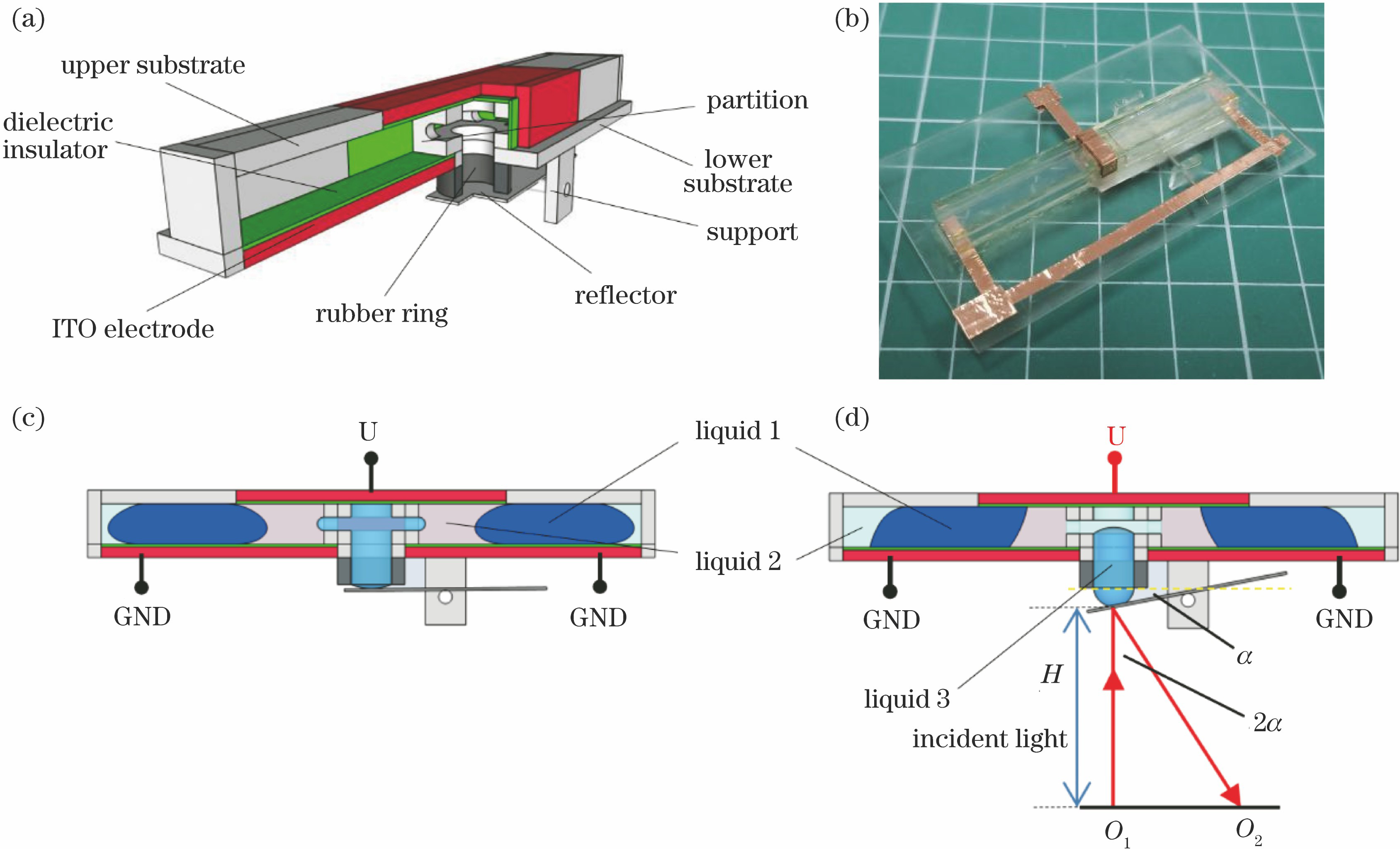
Fig. 1. Schematic structure of optical navigation device. (a) Profile of the device; (b) picture of the device; (c) initial state; (d) applying external voltage
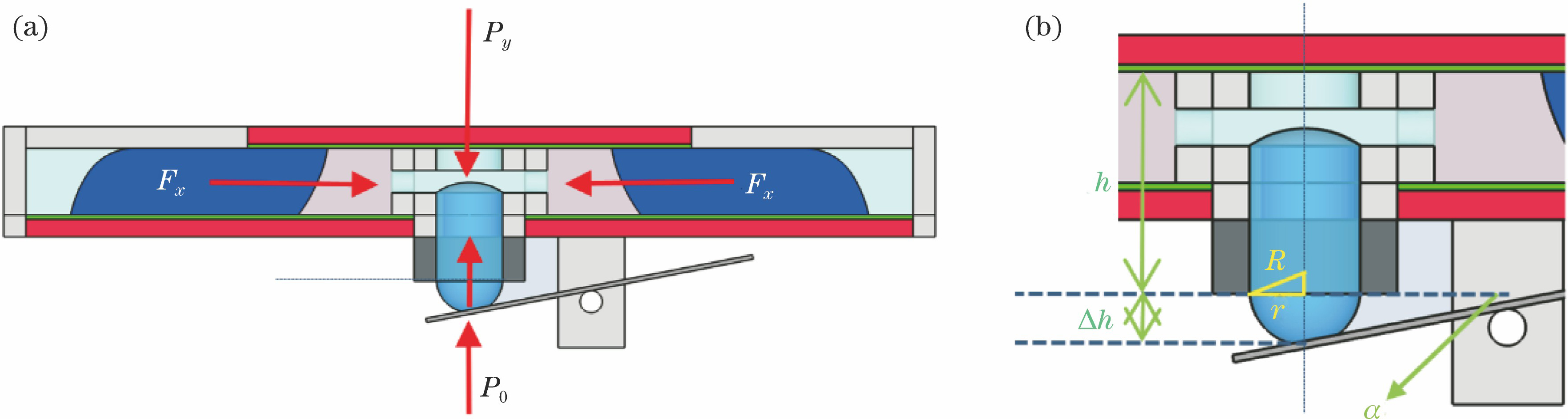
Fig. 2. Analysis of force balance of optical tracking. (a) Equilibrium state when applying external voltage; (b) liquid 3 and mirror contact part
Fig. 3. Results of height change of the liquid 3 under different voltages
Fig. 4. Heightof liquid 3 versus voltage
Fig. 5. Experimental setup of optical tracking angle measurement
Fig. 6. Experimental results of optical tracking angle measurement. (a) Variation of tilt angle of mirror under different voltages; (b) incident beam deflection under different voltages; (c) relationship between optical tracking angle and applied voltage; (d) relationship between deflection angle of incident beam and applied voltage

Set citation alerts for the article
Please enter your email address
© Copyright 2018-2021 | Chinese Laser Press. All Rights Reserved 沪ICP备15018463号-20