• Laser & Optoelectronics Progress
  • Vol. 58, Issue 1, 123001 (2021)
Cheng Jin1, Zhou Shun1, Xu Naitao1、2, Lu Anjiang3, and Liu Weiguo1
Author Affiliations
  • 1School of Photoelectric Engineering, Xi''an Technological University, Xi''an, Shaanxi 710021, China
  • 2China Key System & Integrated Circuit Co., Ltd, Wuxi, Jiangsu 214101, China
  • 3College of Big Data and Information Engineering, Guizhou University, Guiyang, Guizhou 550025, China
  • show less
    DOI: 10.3788/LOP202158.0123001 Cite this Article Set citation alerts
    Cheng Jin, Zhou Shun, Xu Naitao, Lu Anjiang, Liu Weiguo. Low-Cost Two-Dimensional Laser Scanning Projection Technology[J]. Laser & Optoelectronics Progress, 2021, 58(1): 123001 Copy Citation Text show less
    MEMS laser projection module. (a) Actual scanning module; (b) two-dimensional MEMS scanning micromirror chip
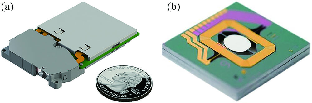
    Fig. 1. MEMS laser projection module. (a) Actual scanning module; (b) two-dimensional MEMS scanning micromirror chip
    Structure of two-dimensional MEMS scanning device
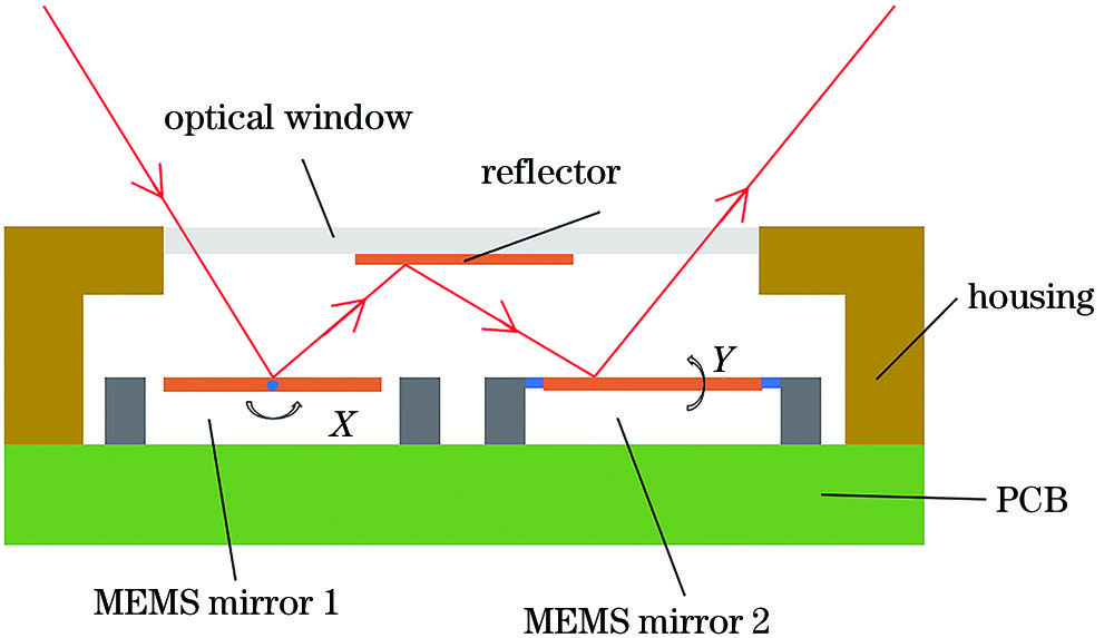
    Fig. 2. Structure of two-dimensional MEMS scanning device
    Structure of one-dimensional electrostatic MEMS scanning micromirror
    Fig. 3. Structure of one-dimensional electrostatic MEMS scanning micromirror
    Rotational resonance mode of MEMS scanning micromirror under different frequencies. (a) 28.186 kHz ;(b) 3.162 kHz
    Fig. 4. Rotational resonance mode of MEMS scanning micromirror under different frequencies. (a) 28.186 kHz ;(b) 3.162 kHz
    Manufacturing process of MEMS scanning micromirror
    Fig. 5. Manufacturing process of MEMS scanning micromirror
    Physical images of MEMS scanning micromirror in different directions. (a) X axis; (b) Y axis
    Fig. 6. Physical images of MEMS scanning micromirror in different directions. (a) X axis; (b) Y axis
    MEMS two-dimensional scanning device module before and after packaging. (a) Before packaging; (b) after packaging
    Fig. 7. MEMS two-dimensional scanning device module before and after packaging. (a) Before packaging; (b) after packaging
    Relationship between voltage and optical angle. (a) X axis; (b) Y axis
    Fig. 8. Relationship between voltage and optical angle. (a) X axis; (b) Y axis
    Optical angle test equipment and Lissajous pattern
    Fig. 9. Optical angle test equipment and Lissajous pattern
    StructureX-axisY-axis
    Chip size/mm×mm×mm4.7×2.2×0.54.7×5.1×0.5
    Mirror size/mm×mm1.2×1.02.9×2.2
    Finger number140400
    Finger gap/μm55
    Finger width/μm55
    Finger thickness/μm4545
    Finger length/μm150300
    Torsional beam/μm×μm580×50400×40
    Table 1. Key parameters of MEMS scanning micromirror
    Cheng Jin, Zhou Shun, Xu Naitao, Lu Anjiang, Liu Weiguo. Low-Cost Two-Dimensional Laser Scanning Projection Technology[J]. Laser & Optoelectronics Progress, 2021, 58(1): 123001
    Download Citation