• Journal of Semiconductors
  • Vol. 41, Issue 8, 082001 (2020)
Yixuan Fan1, Le Huang2, Dechao Geng1, and Wenping Hu1
Author Affiliations
  • 1Tianjin Key Laboratory of Molecular Optoelectronic Sciences, Department of Chemistry, School of Science, Tianjin University and Collaborative Innovation Center of Chemical Science and Engineering, Tianjin 300072, China
  • 2School of Materials and Energy, Guangdong University of Technology, Guangzhou 510006, China
  • show less
    DOI: 10.1088/1674-4926/41/8/082001 Cite this Article
    Yixuan Fan, Le Huang, Dechao Geng, Wenping Hu. Controlled growth of Mo2C pyramids on liquid Cu surface[J]. Journal of Semiconductors, 2020, 41(8): 082001 Copy Citation Text show less
    (Color online) Schematic showing the growth of Mo2C pyramids on liquid Cu substrate.
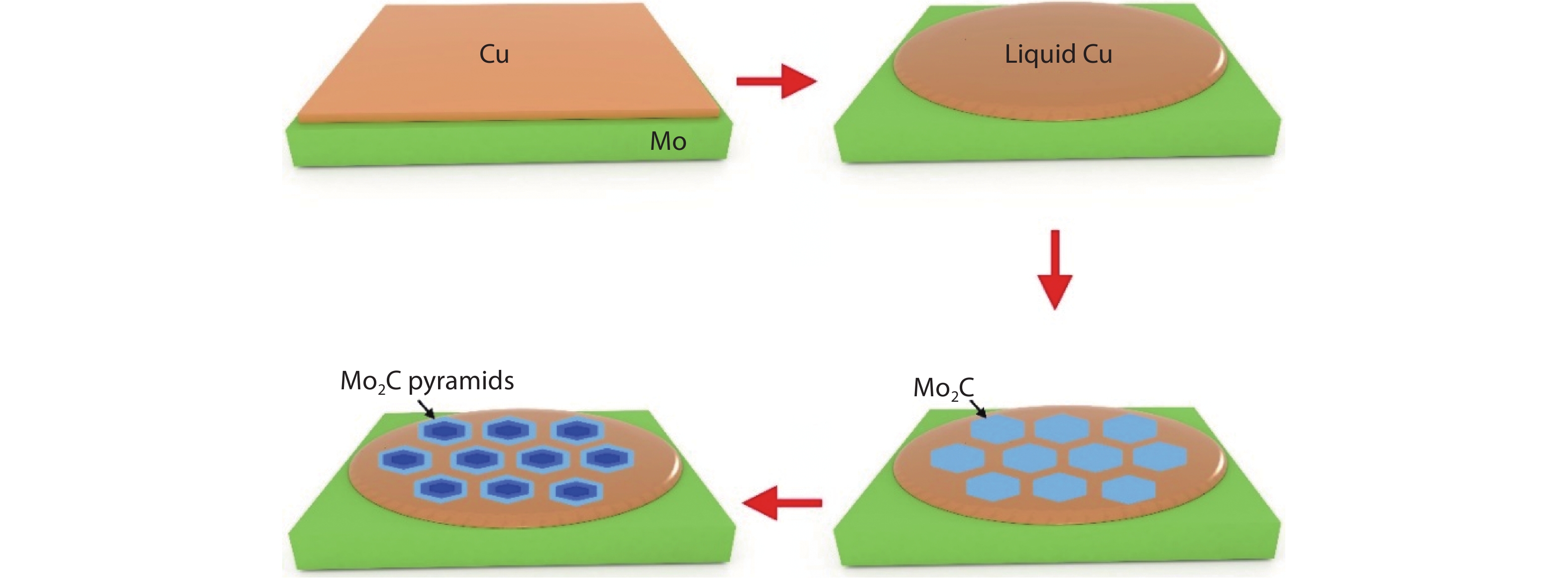
    Fig. 1. (Color online) Schematic showing the growth of Mo2C pyramids on liquid Cu substrate.
    (Color online) Growth and characterization of Mo2C pyramids. (a) Crystal and (b, c) electronic structure of Mo2C from first-principles calculations. (d) Optical images of grown Mo2C pyramids structures on liquid Cu surface. (e, f) XPS spectra of Mo2C flake, indicating existence of Mo and C, respectively. (g–i), AFM images of three typical layered pyramids structures.
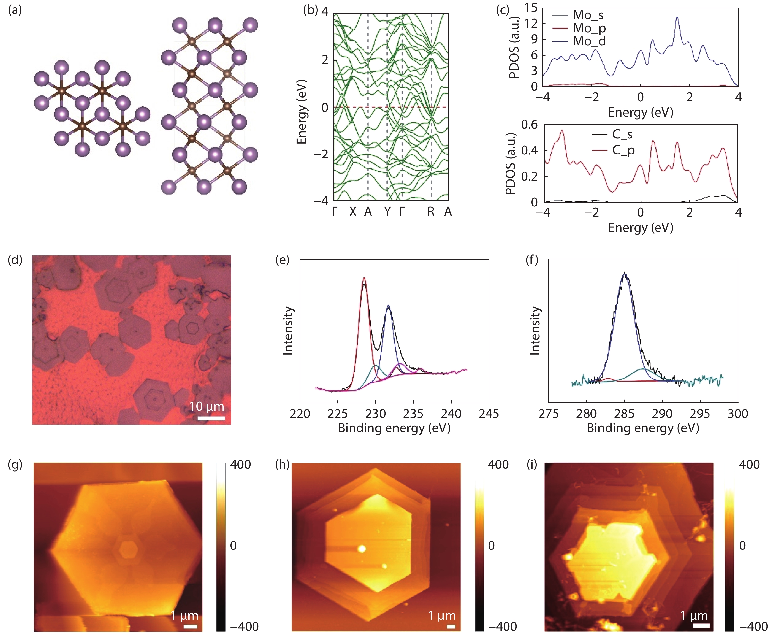
    Fig. 2. (Color online) Growth and characterization of Mo2C pyramids. (a) Crystal and (b, c) electronic structure of Mo2C from first-principles calculations. (d) Optical images of grown Mo2C pyramids structures on liquid Cu surface. (e, f) XPS spectra of Mo2C flake, indicating existence of Mo and C, respectively. (g–i), AFM images of three typical layered pyramids structures.
    (Color online) Further characterization and proposed model of Mo2C pyramid structures. (a) Optical images of grown layered Mo2C structures on liquid Cu surface and SiO2/Si substrate. (b) Raman spectrum of Mo2C flake, having characterized peak at around 650 cm–1. (c, d) Optical image of broken layered Mo2C structure, with bare hexagonal profile of Cu left.
    Fig. 3. (Color online) Further characterization and proposed model of Mo2C pyramid structures. (a) Optical images of grown layered Mo2C structures on liquid Cu surface and SiO2/Si substrate. (b) Raman spectrum of Mo2C flake, having characterized peak at around 650 cm–1. (c, d) Optical image of broken layered Mo2C structure, with bare hexagonal profile of Cu left.
    (Color online) Growth of novel Mo2C pyramid structures. (a) Optical images of the large-area as-grown Mo2C structures on liquid Cu surface and transferred onto SiO2/Si substrate, respectively. (b) AFM image of the single structure, displaying clear layered feature. The inset shows height profile of the structure, showing step feature across the whole flake reflected in thickness. (c–f) Optical images of the growth process of Mo2C structures, showing the time-dependent feature. (g) Schematic diagram illustrates the growth of novel layered Mo2C structures, corresponding to the observations in (c–f).
    Fig. 4. (Color online) Growth of novel Mo2C pyramid structures. (a) Optical images of the large-area as-grown Mo2C structures on liquid Cu surface and transferred onto SiO2/Si substrate, respectively. (b) AFM image of the single structure, displaying clear layered feature. The inset shows height profile of the structure, showing step feature across the whole flake reflected in thickness. (c–f) Optical images of the growth process of Mo2C structures, showing the time-dependent feature. (g) Schematic diagram illustrates the growth of novel layered Mo2C structures, corresponding to the observations in (c–f).
    (Color online) STEM characterization of Mo2C pyramid. (a) STEM-ADF image of a typical edge region in the Mo2C pyramids structures. (b) Strain field mapping based on the image shown in (a).
    Fig. 5. (Color online) STEM characterization of Mo2C pyramid. (a) STEM-ADF image of a typical edge region in the Mo2C pyramids structures. (b) Strain field mapping based on the image shown in (a).
    Yixuan Fan, Le Huang, Dechao Geng, Wenping Hu. Controlled growth of Mo2C pyramids on liquid Cu surface[J]. Journal of Semiconductors, 2020, 41(8): 082001
    Download Citation