
Zhengfen Wan, Xi Chen, Min Gu. Laser scribed graphene for supercapacitors[J]. Opto-Electronic Advances, 2021, 4(7): 200079-1
- Opto-Electronic Advances
- Vol. 4, Issue 7, 200079-1 (2021)
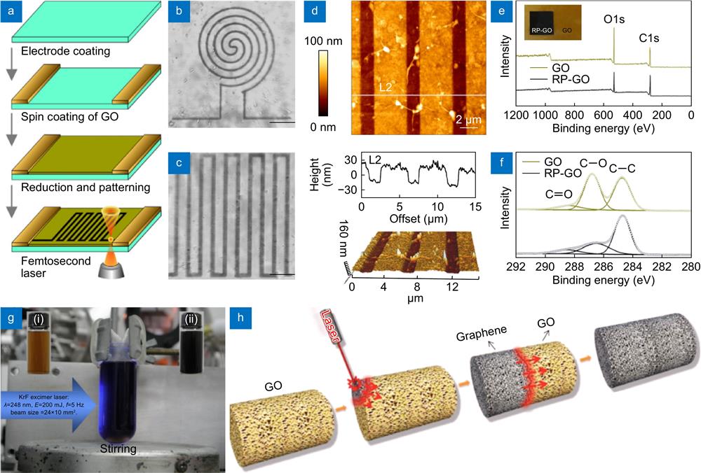
Fig. 1. Illustration of various GO precursors reduced by laser scrbing. (a ) The preparative procedure of LSG microcircuit on GO film. (b–c ) Optical microscopy images of laser patterned microcircuit; Scale bars, 10 μm. (d ) Atomic force microscope (AFM) image of LSG microcircuit on GO film, the height profile along the white line (L2), and its 3D image. (e ) Survey X-ray photoelectron spectra of GO and LSG. Inset is a photograph of a LSG square on a GO film. (f ) C1s x-ray photoelectron spectroscopy (XPS) spectra of GO and LSG. (g ) The experimental setup of pulsed laser reduction system. The inset is optical images of GO solution (15 mL 0,1 mg/mL) before (i) and after (ii) pulsed laser irradiation. (h ) Schematic illustration of the GO aerogel treated by laser for the preparation of graphene bulks. Figures reproduced with permission from: (a–e) ref.33 and (g) ref.43, Elsevier; (h) ref.45, John Wiley and Sons.
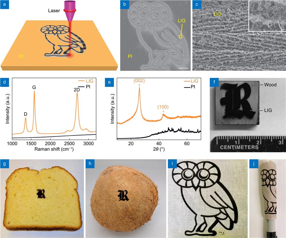
Fig. 2. (a ) Schematic illustration of laser patterning on polyimide (PI). (b–c ) SEM image of LSG on the PI substrate (b) with scale bar 1 mm and its enlarged SEM image with scale bar 10 μm (c). Inset is the corresponding SEM image with higher magnification, scale bar 1 μm. (d–e ) Raman spectrum (d) and X-ray diffraction (XRD) (e) of a LSG and the PI film. (f ) A photo of LSG on pine wood. (g ) The letter “R” in LSG induced from bread. (h ) Picture of LSG patterned into an “R” on a coconut (2 cm tall). (i–j ) LSG on cloth in the shape of an owl (60 mm in height) (i) and the wrapped cloth (j). Figure reproduced with permission from: (a–e) ref.48, Springer Nature; (f) ref.52, John Wiley and Sons; (g–j) ref.53, American Chemical Society.
Fig. 3. (a ) Schematic illustration of the fabrication of LSG based supercapacitors with sandwiched structures. (b ) Schematic diagram of the preparation process for an in-plane LSG supercapacitor. Figure reproduced with permission from: (a) ref.69 , AAAS; (b) ref.70 , Springer Nature.
Fig. 4. (a ) Synthetic scheme for the preparation of boron-doped LSG and its fabrication of supercapacitor. (b ) The B1s spectrum of XPS spectra of PI/H3BO3 sheet and boron-doped LSG. (c–d ) Cyclic voltammetry curves (c) and galvanostatic charge-discharge curves (d) of LSG SC and boron-doped LSG SC with different H3BO3 loadings. Figure reproduced with permission from ref.72 , American Chemical Society.
Fig. 5. (a ) Schematic showing the insertion of CNTs between GO layers to effectively inhibit the restacking and the fabrication process for the flexible supercapacitor (LSG/CNTs SC). (b ) Digital photographs of an assembled SC. (d–e ) Cyclic voltammetry curves (d), charge-discharge curves (e) and for LSG SCs, LSG/CNTs SCs with different diameters. (f ) Schematic illustration and photos of fabrication of LSG/Au supercapacitors onto a paper substrate. (g ) The SEM image of LSG/Au microelectrodes. (h–i ) Comparison of electrochemical performances of both the LSG/Au SCs and LSG SCs: cyclic voltammetry curves (h) and galvanostatic charge/discharge curves (i). Figure reproduced with permission from: (a–e) ref.73, Elsevier; (f–i) ref.71, Royal Society of Chemistry.
Fig. 6. (a ) Schematic diagram of a high-voltage planar SC based on laser scribed graphene. (b ) Schematic illustration and the related strain property of the kirigami-inspired electrodes with different geometric unit numbers (scale bar 1 cm). (c ) Illustration of stacked LSG-SCs in series and parallel circuits and its structure. (d ) Schematic diagram of the direct laser reduction of GO fiber for the bamboo-like series of GO-LSG fiber. (e ) Bio-inspired fractal electrode design of Hilbert fractal structures. (f ) Schematic structure of the Hilbert fractal electrode supercapacitor. Figure reproduced with permission from: (a) ref.74, American Chemical Society; (b) ref.96, Springer Nature; (c) ref.34, American Chemical Society; (d) ref.98, Royal Society of Chemistry; (e−f) ref.75, under a Creative Commons Attribution 4.0 International License.
Fig. 7. Schematic and structural illustration of LSG/Ni-CAT MOF. (a ) An in-plane interdigital LSG pattern. (b ) Solvothermal growth of Ni-CAT MOF nanorods. (c ) Structure of LSG/Ni-CAT MOF. (d ) SEM images of LSG and LSG/Ni-CAT MOFs, respectively. (e ) Cyclic voltammetry comparison of bare LSG and LSG/Ni-CAT MOF. (f ) Galvanostatic charge/discharge curves of bare LSG and LSG/Ni-CAT MOF. Figure reproduced with permission from ref.35, John Wiley and Sons.
Fig. 8. (a ) Schematic illustration of the deposition process of laser-oxidized Fe3O4 nanoparticles anchored on porous laser scribed graphene by direct laser writing technique. (b–c ) SEM images of (b ) 3D porous LSG and (c ) 3D LSG/Fe3O4 nanoparticle composite. (d ) CV curves of LSG/Fe3O4-X at 5 mV·s−1 (e ) GCD profiles of LSG/Fe3O4-X at 1 mA·cm−2 . Figure reproduced with permission from ref.77, Elsevier.
Fig. 9. (a ) Schematic of the fabrication steps for the LSG supercapacitor on textile. (b ) CV measurements on LSG supercapacitors without encapsulation under different stretchable conditions for a scan rate of 5 V·s−1. (c ) Capacitance retention under the maximum stretchable condition of 200% along the uniaxial direction for a scan rate of 5 V·s−1. Figure reproduced with permission from ref.112, under a Creative Commons Attribution 4.0 International License.
Fig. 10. (a ) Schematic of experimental setup using a 405 nm laser in SEM. (b ) Fabrication of integrated micro-supercapacitors on a GO film using fs laser processing. (c–d ) LSG electrode arrays maintain high resolution with a spacing of ~2 μm. (e–f ) CV profiles of fs MSC with the interelectrode spacing of (e) 2 μm and (f) 550 μm. (g ) Two-photon-induced 3D graphene micro-supercapacitor using a fs laser. Figure reproduced with permission from: (a) ref.117 and (b–f) ref.80, American Chemical Society; (g) ref.81, under a Creative Commons Attribution 4.0 International License.
Fig. 11. (a ) Schematic of the integrated energy storage with silicon solar cells. (b ) Schematic illustration of the self-powered photodetection system including a commercial solar panel, a SC, and a ZnO-based photodetector. (c ) Self-discharge curve of the SC after being charged by the solar panel for 1 minute. (d ) Photocurrent curves of the photodetector driven by the SC. (e ) Schematic illustration for the fabrication of a wireless charging and storage integrated device. (f ) Potential change of the integrated SC charged by the wireless circuit placed on a commercial wireless charger. (g ) Serially connected thermally chargeable SC modules whose ends are colored in black and silvery-white to create temperature differences under solar radiation. (h ) The steady-state voltage of 8 thermally chargeable SC modules as a function of ΔT . Figure reproduced with permission from: (a) ref.122, AIP Publishing; (b–d) ref.124, Elsevier; (e, f) ref.57, American Chemical Society; (g, h) ref.125, Elsevier.
| |||||||||||||||||||||||||||||||||||||||||||||||||||||||||||||||||||||||||||||||||||||||||||||||||||||||||||||||||||||||||||||||||||||||||||||||||||||||||||||||||||||||||||||||||||||||||||||||||||||||||||||||||||||||||||||||||||||||||||||||||||||||||||||||||||||
Table 1. The performances of laser scribed graphene based supercapacitors


Set citation alerts for the article
Please enter your email address

© Copyright 2018-2021 | Chinese Laser Press. All Rights Reserved 沪ICP备15018463号-20