
Hua Lu, Xuetao Gan, Dong Mao, Jianlin Zhao. Graphene-supported manipulation of surface plasmon polaritons in metallic nanowaveguides[J]. Photonics Research, 2017, 5(3): 162
- Photonics Research
- Vol. 5, Issue 3, 162 (2017)
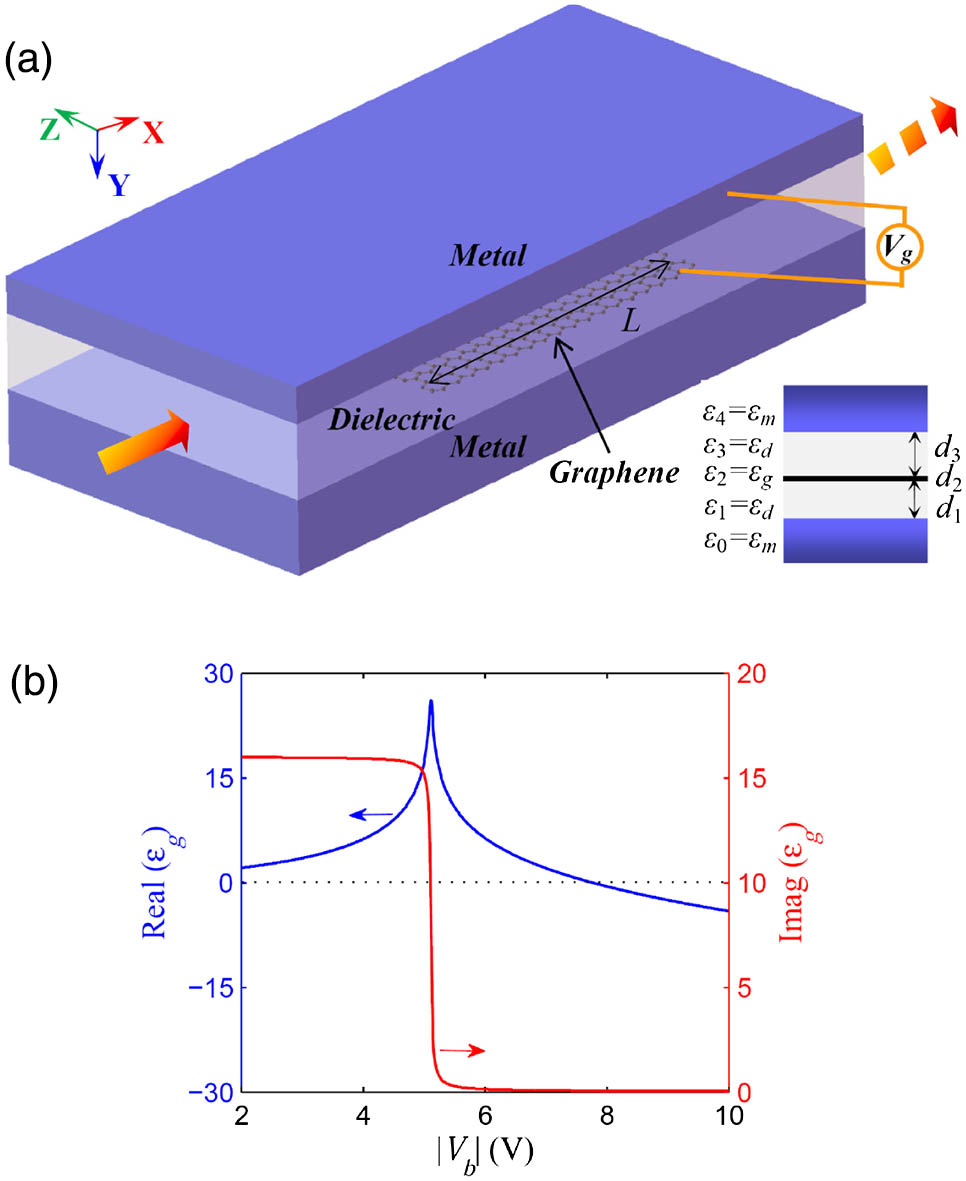
Fig. 1. (a) Schematic diagram of the graphene-supported MDM plasmonic waveguide. An external gate voltage V g d 1 d 3 ϵ d = 2.25 d 2 L ϵ g | V b | d 1 = 45 nm d 3 = 5 nm
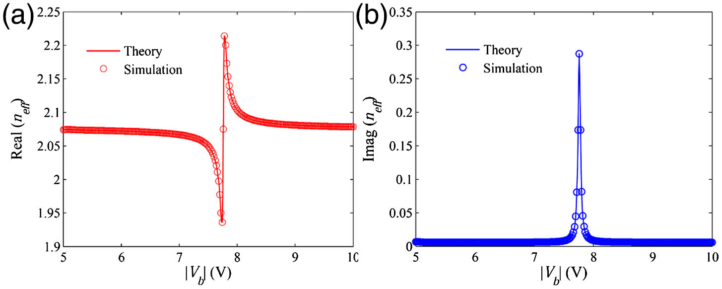
Fig. 2. (a) Real and (b) imaginary parts of ERI (n eff λ = 1.49 μm d 1 = 45 nm d 3 = 5 nm
Fig. 3. (a)–(d) Normalized electric field and magnetic field profiles in the MDM waveguide at λ = 1.49 μm | V b | = 6
Fig. 4. Transmission spectra in the graphene-supported MDM plasmonic waveguide [shown in Fig. 1(a) ] when | V b | = 6 d 1 = 45 nm d 3 = 5 nm L = 670 nm
Fig. 5. (a) Schematic diagram of the graphene-supported MDM plasmonic waveguide with the double side-coupled stubs. The inset shows the cross-section diagram of the plasmonic waveguide. l 1 w 1 l 2 w 2 | V b | = 6 V | V b | = 7.76 V d 1 = 45 nm d 3 = 5 nm l 1 = 130 nm w 1 = 50 nm l 2 = 190 nm w 2 = 50 nm L = 670 nm
Fig. 6. (a)–(d) Normalized electric field and magnetic field distributions at λ = 1.49 μm | V b | = 6
Fig. 7. ER of the EOM as a function of the carrier mobility μ

Set citation alerts for the article
Please enter your email address
© Copyright 2018-2021 | Chinese Laser Press. All Rights Reserved 沪ICP备15018463号-20