Abstract
We investigate the electrically controlled light propagation in the metal–dielectric–metal plasmonic waveguide with a sandwiched graphene monolayer. The theoretical and simulation results show that the propagation loss exhibits an obvious peak when the permittivity of graphene approaches an epsilon-near-zero point when adjusting the gate voltage on graphene. The analog of electromagnetically induced transparency (EIT) can be generated by introducing side-coupled stubs into the waveguide. Based on the EIT-like effect, the hybrid plasmonic waveguide with a length of only 1.5 μm can work as a modulator with an extinction ratio of , which is 2.3 times larger than the case without the stubs. The active modulation of surface plasmon polariton propagation can be further improved by tuning the carrier mobility of graphene. The graphene-supported plasmonic waveguide system could find applications for the nanoscale manipulation of light and chip-integrated modulation.1. INTRODUCTION
The miniaturization and integration of optical and optoelectronic devices have been part of the development of the information technology to process the explosively growing data. However, it is particularly difficult for traditional optical devices to realize the ultrasmall size and ultrahigh integration owing to the classical diffraction limit of light. Surface plasmon polaritons (SPPs) are electromagnetic waves coupled to free electron oscillations traveling along the metal–dielectric interface, which are considered one of the most cutting-edge and promising technologies for the realization of highly integrated optical circuits because of their capacity to manipulate light at nanoscale and overcome the diffraction limit of light [1–3]. Until now, a large number of SPP-based functional components have been investigated numerically and experimentally for the generation, propagation, manipulation, and detection of light signals [2–12]. Among them, metal–dielectric–metal (MDM) waveguides have very strong light confinement with the acceptable lengths for SPP propagation [4,7,12–14]. The excellent properties of the MDM waveguide facilitate the chip-integrated optical devices with relatively easy fabrication using existing state-of-the-art tools [13,14]. On the basis of the MDM waveguides, various nanoplasmonic devices were proposed, such as nanolasers [15], Bragg filters [16,17], wavelength demultiplexers [18], splitters [19], switchers [20], dipolar emitters [21], and detectors [4]. These MDM waveguide devices will contribute to the realization of chip-integrated optical circuits [3]. The active control of SPP propagation in the MDM waveguides is of great importance for exploring active nanoscale optical devices, especially modulators [7].
Graphene, a two-dimensional (2D) material with a single layer of carbon atoms arranged in a honeycomb lattice, has attracted wide attention due to its exceptional optoelectronic properties [22–34]. The unique properties of this 2D material contain the ultrahigh carrier mobility [], extremely wide operating frequency range, versatile tunability by controlling the gate voltage or chemical doping, and compatibility with other photonic elements [23,24]. These properties make graphene a potential answer for the realization of high-performance photonic and optoelectronic devices. Recently, tremendous graphene photonic devices have been proposed, such as chip-integrated detectors [16], slow-light components [25,29], filters [30], polarizers [26], and nanospasers [27]. By exerting the gate voltage on graphene to control the dissipative loss, especially, the active control of light can be simply achieved in the silicon and photonic crystal waveguides [23,28]. The dynamic tunability of graphene absorption offers a promising pathway toward the electro-optic modulation (EOM) for optical signal processing [28]. Light modulation at a visible range in optical cavities with electrical doping graphene was proposed by Yu et al. [35]. The graphene-based active modulation of light was proposed numerically in metal plasmonic waveguide systems [36,37].
Here, we present a method for the active control of the SPP propagation by electrically tuning the graphene monolayer sandwiched in the MDM waveguide. The theoretical calculations show that the propagation attenuation of SPP mode in the MDM waveguide possesses a sharp peak when the permittivity of graphene reaches the epsilon-near-zero (ENZ) point by adjusting the bias voltage on graphene. The results are in excellent agreement with the numerical simulations. The dynamic tunability of graphene contributes to the active modulation of SPP propagation in MDM waveguides. Particularly, the extinction ratio (ER) of EOM can approach in the waveguide with a length of only 1.5 μm, which originates from the generation of the plasmonic analog of electromagnetically induced transparency (EIT). The ER can be further improved by increasing the carrier mobility of graphene. The high-ER modulation of strongly confined SPP propagation in the ultrasmall system provides a new avenue toward the realization of the manipulation and modulation of light at nanoscale.
Sign up for Photonics Research TOC. Get the latest issue of Photonics Research delivered right to you!Sign up now
2. MODEL AND THEORY
As shown in Fig. 1(a), the plasmonic waveguide system consists of a graphene monolayer sandwiched in an MDM waveguide. An external gate voltage is exerted on the graphene. The distance between the graphene and metal film below (above) the dielectric layer is , as depicted in the inset of Fig. 1(a). The thickness and length of graphene layer are and , respectively. The dielectric layer is assumed as silica with the relative permittivity . The metal is selected as silver, whose relative permittivity in the near-infrared region can be described by the well-known Drude model: [38]. Here, stands for the dielectric constant at the infinite frequency. and represent the Drude damping and bulk plasma frequencies, respectively. is the angular frequency of incident light in vacuum. These physical parameters for silver in the frequency of interest can be set as , , and [38]. The optical property of the graphene monolayer in metal-based plasmonic systems can be characterized by the complex-valued surface conductivity, which is quantitatively described by the Kubo formula [36,37]. The surface conductivity of graphene can be written as [39]. Here, corresponding to the intraband transition contribution can be given by where stands for the electron charge, is Boltzmann’s constant, is the temperature, is the reduced Planck’s constant, is the photon frequency in vacuum, and is the chemical potential of graphene. When and , corresponding to the interband transition contribution can be expressed as where represents the momentum relaxation time due to the charge carrier scattering, which is dependent on the carrier mobility and can be described as . The Fermi velocity is [39]. The previous report showed that the carrier mobility of graphene on substrate could reach at room temperature [40]. Here, a moderate carrier mobility [] is set to ensure the credibility of results [41]. The chemical potential can be described as [42]. The doping level of graphene depends on the gate voltage and can be expressed as . is the bias voltage of graphene for the modification of . is the voltage offset of graphene caused by the natural doping, and is the applied voltage on graphene. The numerical results can be obtained by using the finite-element method (FEM). In the numerical simulations, the graphene monolayer is rationally assumed as a thin layer with the practical thickness , whose relative permittivity can be described as . The isotropic model for graphene has been effectively employed to investigate plasmonic responses in graphene-involved structures [36,37,39,42–49]. The relative permittivity of graphene is determined by the surface conductivity , which can be tuned by the bias voltage of graphene, as shown in Fig. 1(b).
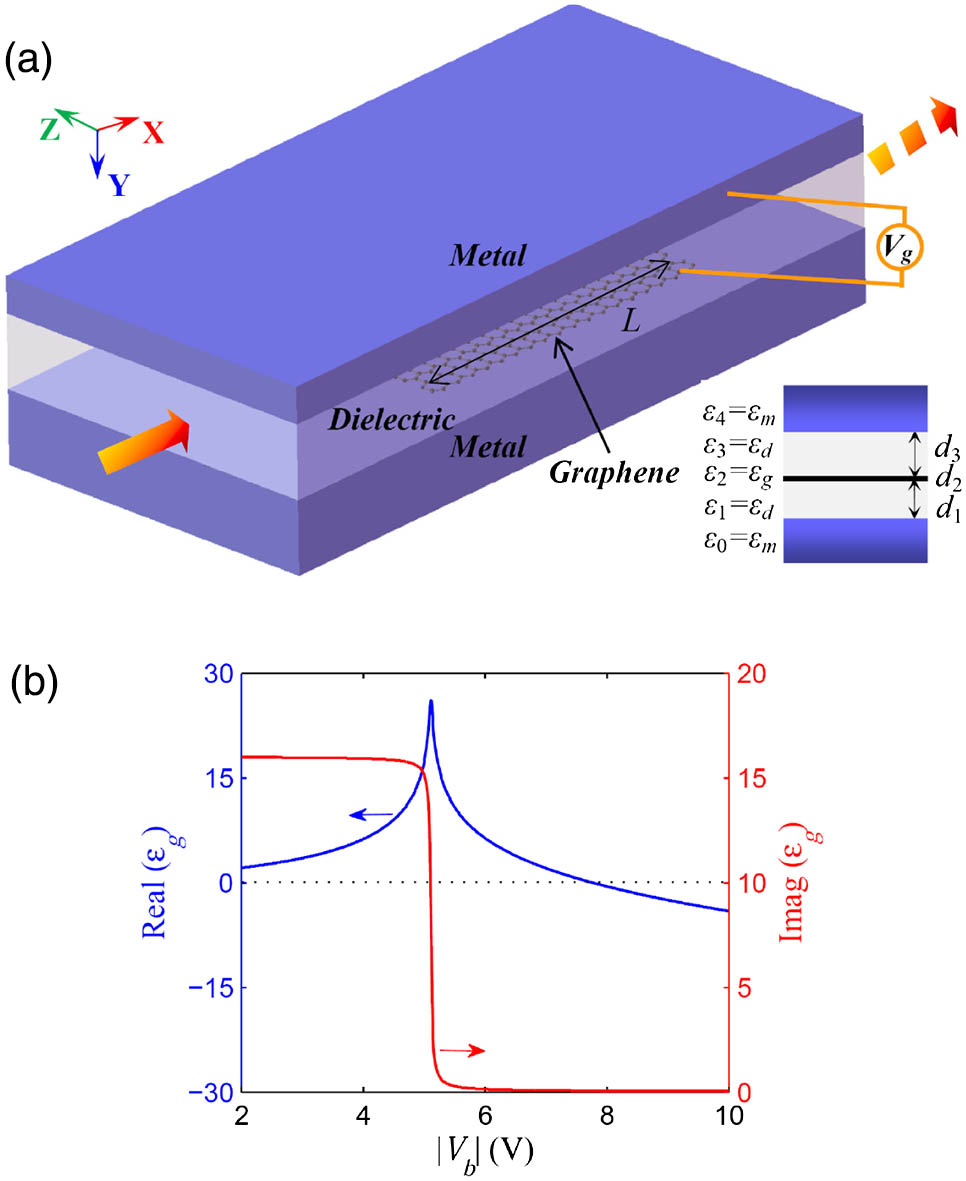
Figure 1.(a) Schematic diagram of the graphene-supported MDM plasmonic waveguide. An external gate voltage is exerted on the graphene. The inset shows the section-cross profile of the waveguide with graphene. Here, () represents the distance between the graphene and metal film below (above) the dielectric layer (silica, ). and are the thickness and length of graphene, respectively. (b) Real and imaginary parts of the relative permittivity of graphene with the different bias voltages at the wavelength of 1.49 μm in the waveguide with and .
When the TM-polarized light is coupled into the MDM waveguide, the SPP wave can be excited at the metal/dielectric interfaces and propagate along the waveguide [19]. The inset of Fig. 1(a) shows the metal–silica–graphene–silica–metal waveguide structure. Derived from Maxwell’s equations, the electric and magnetic fields in the waveguide can be written as and , respectively [50]. Here, stands for the propagation constant of light in the waveguide, is the free-space permeability, and is the speed of light in the vacuum. According to the continuity of tangential fields for and at the interfaces between the metal, silica, and graphene layers, the characteristic equations of light propagation in the waveguide can be described as follows
We assume , , and , as shown in the inset of Fig. 1(a). is the wave number of incident light in the vacuum. is the wavelength of incident light. is the effective refractive index (ERI) of guided mode. The dispersion characteristics of plasmonic modes in the MDM waveguide can be obtained by solving the equations. From the equations, we can see that the dispersion characteristics are dependent on the surface conductivity of graphene, which can be controlled by the bias voltage .
3. RESULTS AND ANALYSIS
We theoretically calculate the ERI with different bias voltages, as shown in Fig. 2. The real part of ERI exhibits a drastic change when approaches 7.76 V at the telecommunication wavelength (e.g., ) in the MDM waveguide with and . Especially, the imaginary part of ERI exists as a sharp peak when . As depicted in Fig. 1(b), the permittivity of graphene reaches the ENZ point when . The ENZ effect in graphene was proposed to realize the electro-optic modulators with comparable modulation depth in the metal and slot hybrid waveguides [36,45–49]. The similar active modulation was achieved in graphene-loaded metal plasmonic antennas [37]. The anisotropic model for graphene may affect or weaken the modulation effects [51,52]. However, the isotropic model is efficient for modulation in plasmonic waveguides [49]. The attenuation coefficient of a plasmonic wave can be described as and possesses a relatively low value of when . It will reach the maximum value of when . To verify the theoretical results, we employ the FEM to simulate the dispersion curves of plasmonic mode. As shown in Fig. 2, the numerical simulations are in excellent agreement with the theoretical calculations.

Figure 2.(a) Real and (b) imaginary parts of ERI () of the plasmonic mode at as a function of the bias voltage of graphene in the MDM plasmonic waveguide with and . The curves and circles denote the theoretical and simulation results obtained by the equations and FEM, respectively.
Through the simulations, we plot the profiles of electric and magnetic fields in the metal–silica–graphene–silica–metal waveguide when and 7.76 V, as shown in Fig. 3. It is found that the intensity of the electric field in the graphene sheet is lower than that in the dielectric layer when . However, the electric field will mainly concentrate in the graphene monolayer when approaches 7.76 V. It is worth noting that the power absorbed in the graphene layer is proportional to , which will be significantly enhanced when is close to the ENZ point. This is the reason why the SPP attenuation dramatically increases when is adjusted from 6 to 7.76 V. As depicted in Figs. 3(b) and 3(d), the profiles of the magnetic fields with different gate voltages on graphene are nearly unchanged, which reveals that the plasmonic modes are still supported in the waveguide even if the permittivity of graphene is drastically altered. The dependence of the SPP attenuation on the bias of graphene is beneficial to the electrically controlled modulation of light propagation in the MDM waveguide. Figure 4 shows the transmission spectra in the graphene-supported MDM waveguide with a length of 1.5 μm when and 7.76 V. Here, the length of a graphene sheet is set as . It is found that the transmission spectrum of the plasmonic wave in the waveguide possesses a sharp dip (with a spectral width of 6 nm) at the wavelength of 1.49 μm when , resulting in the ER of 6.8 dB for the modulation of SPP propagation.
Figure 3.(a)–(d) Normalized electric field and magnetic field profiles in the MDM waveguide at when and 7.76 V.
Figure 4.Transmission spectra in the graphene-supported MDM plasmonic waveguide [shown in Fig. 1(a)] when and 7.76 V. The inset shows the transmission as a function of the bias voltage in the waveguide with , , and .
Subsequently, we introduce double side-coupled stubs with the distance into the MDM waveguide, as shown in Fig. 5(a). The depth and width of the stub 1 (stub 2) are denoted by and ( and ), respectively. The geometrical parameters are set as , , , , , , and . The simulation results in Fig. 5(b) show that a transparency peak appears at in the center of a broad transmission dip when . The transmission spectra in the MDM waveguide with only stub 1 and stub 2, respectively, exhibit the obvious dips at and 1.75 μm, which contribute to the broad transmission dip. The stubs-induced transparency in the waveguide is regarded as a plasmonic analog of EIT in quantum systems [53]. The generation of the transparency peak can be attributed to the constructive interference of transmission waves passing through the double stubs, giving rise to a Fabry–Perot resonance [54]. Thus, the high EIT-like peak can work as the “on” state for optical modulation, which will rapidly decrease with the increase of the bias voltage. As shown in Fig. 5(c), a transmission dip occurs at in the EIT-like transparency window when approaches 7.76 V, which can be treated as the “off” state of the modulation. The inset of Fig. 5(c) illustrates that the maximal ER of the on/off states can approach at , which is excellent for chip-scale modulators with a length of only 1.5 μm. The ER of SPP propagation in the MDM waveguide with the stubs is about 2.3 times larger than the case without the stubs. To clarify the light modulation in the waveguide, we plot the electric and magnetic fields at when and 7.76 V. In Figs. 6(a) and 6(b), we can see that the plasmonic Fabry–Perot resonance is established in the waveguide between the stubs when , which verifies the above analysis of EIT-like effect. Due to the low electric field and weak absorption in graphene, the incident light can effectively pass through the MDM waveguide. When , the high intensity of electric field in graphene and the drastic increase of SPP attenuation in the waveguide will weaken the Fabry–Perot resonance and prohibit the SPP propagation through the waveguide, as shown in Figs. 6(c) and 6(d).
Figure 5.(a) Schematic diagram of the graphene-supported MDM plasmonic waveguide with the double side-coupled stubs. The inset shows the cross-section diagram of the plasmonic waveguide. and ( and ) stand for the height and width of the stub 1 (stub 2), respectively. (b) Transmission spectra in the graphene-supported MDM plasmonic waveguide with the stub 1, stub 2, and double stubs when . (c) Transmission spectra in the waveguide with the double stubs when . The inset shows the ER of the modulation at different wavelengths. Here, , , , , , , and .
Figure 6.(a)–(d) Normalized electric field and magnetic field distributions at in the MDM plasmonic waveguide when and 7.76 V.
Finally, we investigate the dependence of SPP modulation on the carrier mobility of graphene. The transmission spectral dips in the MDM waveguides drop gradually with the increase of . As shown in Fig. 7, the ER increases with , revealing that the higher quality of graphene will further improve the ER of the modulation. For instance, the ER can reach when in the waveguide with the stubs. By adjusting the loss rates in resonator–graphene systems, the critical coupling can be used to realize the total light absorption in graphene [55]. The SPP propagation loss in the metallic waveguide is dependent on . When approaches , the ER can be further improved and exceed 33 dB. The high-performance EOM in the nanoscale waveguide is favorable for chip-integrated signal processing. We believe our results will provide new pathways for the realization of modulators based on other ENZ materials in metallic waveguides [56].
Figure 7.ER of the EOM as a function of the carrier mobility of graphene in the MDM plasmonic waveguide without and with the double side-coupled stubs.
4. CONCLUSIONS
We have proposed graphene-supported MDM waveguides for the electrical control of high confined SPP propagation. The theoretical and simulation results illustrate that the propagation attenuation of the plasmonic mode in the waveguide is strongly dependent on the voltage applied on graphene, and possesses a maximum at the ENZ point of graphene permittivity. The voltage-controlled plasmonic attenuation contributes to the active modulation of SPP propagation at nanoscale. Especially, by properly etching double side-coupled stubs in the metallic waveguide, the ER of the plasmonic modulation can approach by means of the generation of a plasmonic EIT-like effect, which is 2.3 times larger than the case without side-coupled stubs. The ER can be further improved by increasing the carrier mobility of graphene. The proposed graphene-supported plasmonic waveguide will facilitate the highly integrated optical devices for signal processing, especially graphene modulators.
References
[1] W. Barnes, A. Dereux, T. Ebbesen. Surface plasmon subwavelength optics. Nature, 424, 824-830(2003).
[2] D. Gramotnev, S. Bozhevolnyi. Plasmonics beyond the diffraction limit. Nat. Photonics, 4, 83-91(2010).
[3] V. Sorger, R. Oulton, R. Ma, X. Zhang. Toward integrated plasmonic circuits. MRS Bull., 37, 728-738(2012).
[4] P. Neutens, P. Van Dorpe, I. De Vlaminck, L. Lagae, G. Borghs. Electrical detection of confined gap plasmons in metal-insulator-metal waveguides. Nat. Photonics, 3, 283-286(2009).
[5] Q. Gan, Y. J. Ding, F. J. Bartoli. ‘Rainbow’ trapping and releasing at telecommunication wavelengths. Phys. Rev. Lett., 102, 056801(2009).
[6] P. Berini, A. Olivieri, C. Chen. Thin Au surface plasmon waveguide Schottky detectors on p-Si. Nanotechnology, 23, 444011(2012).
[7] A. Melikyan, L. Alloatti, A. Muslija, D. Hillerkuss, P. Schindler, J. Li, R. Palmer, D. Korn, S. Muehlbrandt, D. Thourhout, B. Chen, R. Dinu, M. Sommer, C. Koos, M. Kohl, W. Freude, J. Leuthold. High-speed plasmonic phase modulators. Nat. Photonics, 8, 229-233(2014).
[8] H. Ren, X. Li, Q. Zhang, M. Gu. On-chip noninterference angular momentum multiplexing of broadband light. Science, 352, 805-809(2016).
[9] B. Fan, F. Liu, X. Wang, Y. Li, K. Cui, X. Feng, Y. Huang. Integrated sensor for ultra-thin layer sensing based on hybrid coupler with short-range surface plasmon polariton and dielectric waveguide. Appl. Phys. Lett., 102, 061109(2013).
[10] C. Zhang, C. Min, L. Du, X. Yuan. Perfect optical vortex enhanced surface plasmon excitation for plasmonic structured illumination microscopy imaging. Appl. Phys. Lett., 108, 201601(2016).
[11] J. Chen, Z. Li, X. Zhang, J. Xiao, Q. Gong. Submicron bidirectional all-optical plasmonic switches. Sci. Rep., 3, 1451(2013).
[12] Z. Chen, H. Li, S. Zhan, B. Li, Z. He, H. Xu, M. Zheng. Tunable high quality factor in two multimode plasmonic stubs waveguide. Sci. Rep., 6, 24446(2016).
[13] J. Dionne, L. Sweatlock, H. Atwater, A. Polman. Plasmon slot waveguides: towards chip-scale propagation with subwavelength scale localization. Phys. Rev. B, 73, 035407(2006).
[14] H. Choo, M. Kim, M. Staffaroni, T. Seok, J. Bokor, S. Cabrini, P. Schuck, M. Wu, E. Yablonovitch. Nanofocusing in a metal-insulator-metal gap plasmon waveguide with a three-dimensional linear taper. Nat. Photonics, 6, 838-844(2012).
[15] M. Hill, M. Marell, E. Leong, B. Smalbrugge, Y. Zhu, M. Sun, P. Veldhoven, E. Geluk, F. Karouta, Y. Oei, R. Nötzel, C. Ning, M. Smit. Lasing in metal-insulator-metal sub-wavelength plasmonic waveguides. Opt. Express, 17, 11107-11112(2009).
[16] H. Lu, X. Liu, D. Mao, L. Wang, Y. Gong. Tunable band-pass plasmonic waveguide filters with nanodisk resonators. Opt. Express, 18, 17922-17927(2010).
[17] P. Neutens, L. Lagae, G. Borghs, P. Dorpe. Plasmon filters and resonators in metal-insulator-metal waveguides. Opt. Express, 20, 3408-3423(2012).
[18] F. Hu, H. Yi, Z. Zhou. Wavelength demultiplexing structure based on arrayed plasmonic slot cavities. Opt. Lett., 36, 1500-1502(2011).
[19] G. Veronis, S. Fan. Bends and splitters in metal-dielectric-metal subwavelength plasmonic waveguides. Appl. Phys. Lett., 87, 131102(2005).
[20] C. Min, G. Veronis. Absorption switches in metal-dielectric-metal plasmonic waveguides. Opt. Express, 17, 10757-10766(2009).
[21] R. McCarron, W. Dickson, A. Krasavin, G. Wurtz, A. Zayats. Dipolar emission in trench metal-insulator-metal waveguides for short-scale plasmonic communications: numerical optimization. J. Opt., 16, 114006(2014).
[22] A. Geim, K. Novoselov. The rise of graphene. Nat. Mater., 6, 183-191(2007).
[23] M. Liu, X. Yin, E. Ulin-Avila, B. Geng, T. Zentgraf, L. Ju, F. Wang, X. Zhang. A graphene-based broadband optical modulator. Nature, 474, 64-67(2011).
[24] X. Gan, R. Shiue, Y. Gao, I. Meric, T. F. Heinz, K. Shepard, J. Hone, S. Assefa, D. Englund. Chip-integrated ultrafast graphene photodetector with high responsivity. Nat. Photonics, 7, 883-887(2013).
[25] H. Lu, C. Zeng, Q. Zhang, X. Liu, M. Hossain, P. Reineck, M. Gu. Graphene-based active slow surface plasmon polaritons. Sci. Rep., 5, 8443(2015).
[26] Q. Bao, H. Zhang, B. Wang, Z. Ni, C. Lim, Y. Wang, D. Tang, K. Loh. Broadband graphene polarizer. Nat. Photonics, 5, 411-415(2011).
[27] V. Apalkov, M. Stockman. Proposed graphene nanospasers. Light Sci. Appl., 3, e191(2014).
[28] X. Gan, R. Shiue, Y. Gao, K. Mak, X. Yao, L. Li, A. Szep, D. Walker, J. Hone, T. Heinz, D. Englund. High-contrast electrooptic modulation of a photonic crystal nanocavity by electrical gating of graphene. Nano Lett., 13, 691-696(2013).
[29] R. Hao, X. Peng, E. Li, Y. Xu, J. Jin, X. Zhang, H. Chen. Improved slow light capacity in graphene-based waveguide. Sci. Rep., 5, 15335(2015).
[30] B. Shi, W. Cai, X. Zhang, Y. Xiang, Y. Zhan, J. Geng, M. Ren, J. Xu. Tunable band-stop filters for graphene plasmons based on periodically modulated graphene. Sci. Rep., 6, 26796(2016).
[31] H. Jussila, H. Yang, N. Granqvist, Z. Sun. Surface plasmon resonance for characterization of large-area atomic-layer graphene film. Optica, 3, 151-158(2016).
[32] Z. Li, W. Liu, H. Cheng, S. Chen, J. Tian. Tunable dual-band asymmetric transmission for circularly polarized waves with graphene planar chiral metasurfaces. Opt. Lett., 41, 3142-3145(2016).
[33] W. Liu, B. Wang, S. Ke, C. Qin, H. Long, K. Wang, P. Lu. Enhanced plasmonic nanofocusing of terahertz waves in tapered graphene multilayers. Opt. Express, 24, 14765-14780(2016).
[34] H. Lu, X. Gan, B. Jia, D. Mao, J. Zhao. Tunable high-efficiency light absorption of monolayer graphene via Tamm plasmon polaritons. Opt. Lett., 41, 4743-4746(2016).
[35] R. Yu, V. Pruneri, F. J. G. de Abajo. Resonant visible light modulation with graphene. ACS Photon., 2, 550-558(2015).
[36] J. Shin, J. Kim, J. Kim. Graphene-based hybrid plasmonic modulator. J. Opt., 17, 125801(2015).
[37] R. Yu, V. Pruneri, F. Abajo. Active modulation of visible light with graphene-loaded ultrathin metal plasmonic antennas. Sci. Rep., 6, 32144(2016).
[38] P. Johnson, R. Christy. Optical constants of the noble metals. Phys. Rev. B, 6, 4370-4379(1972).
[39] P. Chen, A. Alù. Atomically thin surface cloak using graphene monolayers. ACS Nano, 5, 5855-5863(2011).
[40] J. Chen, C. Jang, S. Xiao, M. Ishigami, M. Fuhrer. Intrinsic and extrinsic performance limits of graphene devices on SiO2. Nat. Nanotechnol., 3, 206-209(2008).
[41] S. Thongrattanasiri, F. Koppens, F. Abajo. Complete optical absorption in periodically patterned graphene. Phys. Rev. Lett., 108, 047401(2012).
[42] A. Vakil, N. Engheta. Transformation optics using graphene. Science, 332, 1291-1294(2011).
[43] X. He, H. X. Lu. Graphene-supported tunable extraordinary transmission. Nanotechnology, 25, 325201(2014).
[44] J. Christensen, A. Manjavacas, S. Thongrattanasiri, F. Koppens, F. J. G. de Abajo. Graphene plasmon waveguiding and hybridization in individual and paired nanoribbons. ACS Nano, 6, 431-440(2012).
[45] Z. Lu, W. Zhao. Nanoscale electro-optic modulators based on graphene-slot waveguides. J. Opt. Soc. Am. B, 29, 1490-1496(2012).
[46] J. Gosciniak, D. Tan. Graphene-based waveguide integrated dielectric-loaded plasmonic electro-absorption modulators. Nanotechnology, 24, 185202(2013).
[47] J. Gosciniak, D. Tan. Theoretical investigation of graphene-based photonic modulators. Sci. Rep., 3, 01897(2013).
[48] L. Yang, T. Hu, R. Hao, C. Qiu, C. Xu, H. Yu, Y. Xu, X. Jiang, Y. Li, J. Yang. Low-chirp high-extinction-ratio modulator based on graphene-silicon waveguide. Opt. Lett., 38, 2512-2515(2013).
[49] J. Shin, J. Kim. Broadband silicon optical modulator using a graphene-integrated hybrid plasmonic waveguide. Nanotechnology, 26, 365201(2015).
[50] X. Kong, W. Yan, Z. Li, J. Tian. Optical properties of metal-multi-insulator-metal plasmonic waveguides. Opt. Express, 20, 12133-12146(2012).
[51] M. S. Kwon. Discussion of the epsilon-near-zero effect of graphene in a horizontal slot waveguide. IEEE Photon. J., 6, 1-9(2014).
[52] J. Liu, Y. Zhou, L. Li, P. Wang, A. V. Zayats. Controlling plasmon-induced transparency of graphene metamolecules with external magnetic field. Opt. Express, 23, 12524-12532(2015).
[53] G. Wang, H. Lu, X. Liu. Dispersionless slow light in MIM waveguide based on a plasmonic analogue of electromagnetically induced transparency. Opt. Express, 20, 20902-20907(2012).
[54] H. Lu, X. Liu, D. Mao. Plasmonic analog of electromagnetically induced transparency in multi-nanoresonator-coupled waveguide systems. Phys. Rev. A, 85, 053803(2012).
[55] J. R. Piper, S. Fan. Total absorption in a graphene monolayer in the optical regime by critical coupling with a photonic crystal guided resonance. ACS Photonics, 1, 347-353(2014).
[56] Z. Lu, W. Zhao, K. Shi. Ultracompact electroabsorption modulators based on tunable epsilon-near-zero-slot waveguides. IEEE Photon. J., 4, 735-740(2012).


