• Chinese Optics Letters
  • Vol. 20, Issue 2, 021602 (2022)
Tianju Zhang1、2, Chaocheng Zhou3、4, Jia Lin3、**, and Jun Wang1、2、5、*
Author Affiliations
  • 1Laboratory of Micro-Nano Optoelectronic Materials and Devices, Shanghai Institute of Optics and Fine Mechanics, Chinese Academy of Sciences, Shanghai 201800, China
  • 2Center of Materials Science and Optoelectronic Engineering, University of Chinese Academy of Sciences, Beijing 100049, China
  • 3Department of Physics, Shanghai Key Laboratory of Materials Protection and Advanced Materials in Electric Power, Shanghai University of Electric Power, Shanghai 200090, China
  • 4State Key Laboratory of Advanced Optical Communication Systems and Networks, School of Physics and Astronomy, Shanghai Jiao Tong University, Shanghai 200240, China
  • 5CAS Center for Excellence in Ultra-Intense Laser Science, Shanghai 201800, China
  • show less
    DOI: 10.3788/COL202220.021602 Cite this Article Set citation alerts
    Tianju Zhang, Chaocheng Zhou, Jia Lin, Jun Wang. Effects on the emission discrepancy between two-dimensional Sn-based and Pb-based perovskites[J]. Chinese Optics Letters, 2022, 20(2): 021602 Copy Citation Text show less

    Abstract

    Two-dimensional (2D) Sn-based perovskites are a kind of non-toxic environment-friendly emission material with low photoluminescence quantum yields (PLQYs) and enhanced emission linewidths compared to that of 2D Pb-based perovskites. However, there is no work systematically elucidating the reasons for the differences in the emission properties. We fabricate (BA)2SnI4 and (BA)2PbI4 having different defect densities and different exciton-phonon scattering intensities. We also reveal that 2D Sn-based perovskites have stronger exciton-phonon scattering intensity and higher defects density, significantly broadening the emission linewidth and accelerating the exciton relaxation process, which significantly reduces the PLQY of 2D Sn-based perovskites.

    1. Introduction

    Self-assembled two-dimensional (2D) Ruddlesden–Popper phase organic–inorganic halide perovskites with quantum-well structures have attracted much research attention in optoelectronic devices, lasers, and light-emitting diodes (LEDs) by virtue of their superior features such as enhanced stability, high absorption coefficient, tunable light-emitting wavelength, high color purity, and high exciton binding energy[110]. Its chemical structure formula is (RNH3)2(A)n1BnC3n+1, where R is an alkylor aromatic group, A is an organic cation, B is Pb2+, Sn2+, Ge2+, or other elements, and C is a halogen element[11]. For the 2D perovskites system with n=1, the organic cation layer’s dielectric constant is smaller than that of the inorganic octahedral layer in combination with the inorganic layer’s thickness of about 0.7 nm[1214], which causes the weakened dielectric screening effect and the enhanced spatial confinement effect. These effects greatly weaken the dielectric screening between electron-hole pairs to enhance the Coulomb interaction force between them within the inorganic layer, and thus the exciton dominates the optical transitions in materials[12,1517]. Although 2D Pb-based perovskites are favored in the field of LEDs for display applications and lasers, the element Pb2+ is extremely toxic to the environment, limiting its further development. Compared to Pb2+, Sn2+ is non-toxic and has the most similar ionic radius[18], so the lattice parameters obtained by Sn2+ replacement are, in principle, not severely modified[19,20], which makes Sn-based perovskites expected to replace Pb-based perovskites in the future. At the same time, compared with the 2D Pb-based perovskites LEDs for display applications, the 2D Sn-based perovskites LEDs suffer from the disadvantages of low photoluminescence quantum yields (PLQYs) and enhanced emission linewidths [full width at half-maximum (FWHM)>40nm][21,22]. Although much research points out that Sn-based perovskites are more likely to have a higher density of defect states, due to the oxidation potential of Sn2+/Sn4+(0.15eV) being much lower than that of Pb2+/Pb4+(1.8eV)[23], and numerous optimization strategies proposed to improve their PLQY[20-22,2426], it is still difficult to improve their emission linewidths comparable to that of Pb-based perovskites (FWHM<20nm)[3,5,20,27,28]. There are a variety of factors affecting the emission linewidth of the material, mainly the inhomogeneous broadening caused by the disordered nature of the crystal structure and exciton-defect scattering effect, as well as the homogeneous broadening caused by the electron-phonon scattering effect[2931]. However, no research work exists so far to systematically study these effects affecting emission properties between 2D Pb-based perovskites and 2D Sn-based perovskites under the same experimental conditions and further reveal the differences between them.

    In this work, we have fabricated (A)2SnI4 and (A)2PbI4 [A: n-butylammonium (CH3(CH2)3NH3+(BA+))] using the same method, which has different defect densities and different exciton-phonon scattering intensities. Taking advantage of the temperature-dependent photoluminescence (PL) spectra, transient absorption (TA) spectra, time-dependent PL relaxation kinetics, and PLQY experiments, we also revealed that 2D Sn-based perovskites have stronger exciton-phonon scattering intensity and higher defect-state density relative to 2D Pb-based perovskites, which lead to a significant broadening of the emission linewidth and accelerate the exciton relaxation process of 2D Sn-based perovskites, and these effects reduce the PLQY of 2D Sn-based perovskites. These results can guide further improvement in the emission performance of 2D Sn-based perovskites, in which we should select new structures for organic cation layers with relatively high rigidity to reduce the exciton-phonon scattering intensity and use antioxidants to reduce the defect-state density and thus the energy non-radiative loss.

    2. Results and Discussion

    To explain the physical mechanism affecting the optical properties of 2D Sn-based perovskites, we prepared (BA)2SnI4 and (BA)2PbI4 films by the spin-coating method. The schematic of the hybrid quantum-well structure of (BA)2SnI4 and (BA)2PbI4 crystal structures [Fig. 1(a)] shows the perovskite octahedra sandwiched between organic spacer molecules (BA+). Figure 1 shows the ultraviolet-visible (UV-Vis) absorption, steady-state PL spectroscopy, and PLQY of (BA)2SnI4 and (BA)2PbI4. The inset shows that the optical bandgap of (BA)2SnI4 and (BA)2PbI4 was obtained as 1.97 eV and 2.37 eV by the Tauc-plot method, respectively. The PLQY of (BA)2SnI4 is lower than that of (BA)2PbI4, indicating that the defect density of (BA)2SnI4 is higher than that of (BA)2PbI4. Such defect states might arise from undesirable and uncontrolled conversion of Sn2+ to Sn4+, as the oxidation potential of Sn2+/Sn4+(0.15eV), during the process of sample preparation in a glove box with almost the nitrogen environment, in which there is still a trace amount of oxygen that allows the Sn2+ to oxidize to Sn4+[22,23]. Besides, the oxidation potential of Pb2+/Pb4+ is 1.8 eV, which is more negative than that of Sn2+/Sn4+, making Pb2+ a stable state in (BA)2PbI4. In addition, the FWHM of the normalized PL peak of (BA)2PbI4 is 18.5 nm smaller than that of (BA)2SnI4 (39.2 nm), as shown in Fig. 2. For 2D hybrid organic−inorganic perovskites, there is a trapping-state PL phenomenon due to its lattice being relatively soft. For the existence of two types of trap states, one is the intrinsic self-trapped exciton (STE) state caused by the exciton-phonon coupling, and the other trap state is the extrinsic STE state; the STE state is influenced by the local heterogeneity of the permanent defects lattice, which will sink to a different trapping depth[3234]. These trap states can make the PL peaks deviate from the Gaussian line shape with PL tails in the broad spectral range at the low energy edge. To better fit the PL spectral line shapes of both materials, we used three subpeak fits, where the A peak is the PL of the free exciton, and peaks B and C are the PL of the trap states [Figs. 2(a) and 2(b)]. We found that the percentage of trapping-state PL for (BA)2SnI4 is larger than that of trapping-state PL for (BA)2PbI4, as shown in Fig. 2(c). At the same time, we have tested the time-resolved PL (TRPL) decay kinetics of the PL peak and further performed fitting using two decay exponents [Fig. 2(d)]. We found that the PL lifetime of (BA)2PbI4 is longer than that of (BA)2SnI4, thus further evidencing that the PLQY of (BA)2PbI4 is higher than that of (BA)2SnI4. In summary, we proved that (BA)2SnI4 has a higher defect density relative to (BA)2PbI4. For the (BA)2PbI4, the valence band maximum (VBM) consists of an antibonding hybridization between I (5p states) and Pb2+ (6s states), and the conduction band minimum (CBM) comprises a bonding hybridization between Pb2+ (6p states)[23,35]. For the (BA)2SnI4, the VBM consists of an antibonding hybridization between I (5p states) and Sn2+ (5s states), and the CBM comprises a bonding hybridization between Sn2+ (5p states)[23]. The spin-orbit coupling of the Sn2+ 5p state is lower than that of the Pb2+ 6p state[36], so this lowering of spin-orbit coupling increases the probability of defect states in (BA)2SnI4. In order to further analyze the factors affecting the FWHM, we conducted the temperature-dependent PL spectra to analyze the different physical processes of scattering (Fig. 3).

    Spectral characteristics of (BA)2BI4 (B: Sn/Pb) perovskites. (a) Schematic of the hybrid quantum-well structure of the crystal structure, showing the perovskite octahedra sandwiched between organic spacer molecules (BA+). The UV-visible (UV-Vis) absorption, steady-state photoluminescence (PL) spectra of (b) (BA)2SnI4 and (c) (BA)2PbI4. (d) PLQY of (BA)2SnI4 and (BA)2PbI4.

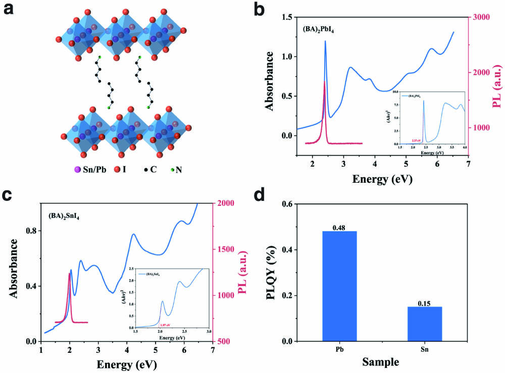
    Figure 1.Spectral characteristics of (BA)2BI4 (B: Sn/Pb) perovskites. (a) Schematic of the hybrid quantum-well structure of the crystal structure, showing the perovskite octahedra sandwiched between organic spacer molecules (BA+). The UV-visible (UV-Vis) absorption, steady-state photoluminescence (PL) spectra of (b) (BA)2SnI4 and (c) (BA)2PbI4. (d) PLQY of (BA)2SnI4 and (BA)2PbI4.

    Analysis of PL characteristics. (a) Multi-peak fit analysis of (BA)2PbI4, (b) multi-peak fit analysis of (BA)2SnI4, (c) percentage of subpeaks of (BA)2PbI4 and (BA)2SnI4, (d) normalized PL decay kinetics.

    Figure 2.Analysis of PL characteristics. (a) Multi-peak fit analysis of (BA)2PbI4, (b) multi-peak fit analysis of (BA)2SnI4, (c) percentage of subpeaks of (BA)2PbI4 and (BA)2SnI4, (d) normalized PL decay kinetics.

    Temperature dependence of the steady-state PL spectra. Contour map of the temperature-dependent steady-state PL spectra of (a) (BA)2SnI4 and (b) (BA)2PbI4. Fitting of the temperature-dependent FWHM of (c) (BA)2SnI4 and (d) (BA)2PbI4. The red fitting line of the data (blue point) is obtained by Eq. (1).

    Figure 3.Temperature dependence of the steady-state PL spectra. Contour map of the temperature-dependent steady-state PL spectra of (a) (BA)2SnI4 and (b) (BA)2PbI4. Fitting of the temperature-dependent FWHM of (c) (BA)2SnI4 and (d) (BA)2PbI4. The red fitting line of the data (blue point) is obtained by Eq. (1).

    The variation of PL FWHM with temperature involves different physical processes of scattering, and the analysis of temperature-dependent PL FWHM is the main means to evaluate the electron-phonon coupling mechanism in various semiconductors[29,30]. Using first-order perturbation theory, the temperature-dependent FWHM can be approximately simplified to a model that contains four scattering mechanisms, as shown in Eq. (1)[37,38]. In the fitting process, the model utilizes a single phonon energy fit, which neglects the feature of the variation of phonon energy with temperature. Therefore, the fitting results have a certain limitation. However, it is helpful as a guide to understand the scattering between excitons and phonons in perovskite materials: Γ(T)=Γ0+γacT+ΓLOeELO/kBT1+ΓimpeEimp/kBT,where the first term Γ0 on the right-hand side of Eq. (1) is the temperature-independent inhomogeneous broadening, which originates from the disordered nature of the crystal structure[29,30]. The second and third terms are temperature-dependent homogeneous broadening due to exciton-acoustic phonon scattering interactions and exciton-longitudinal optical (LO) phonon scattering interactions, where γac is the coupling strength of the exciton-acoustic phonon scattering, ΓLO is the Fröhlich coupling strength of the exciton scattering with LO phonons, and ELO is the energy of the LO phonon. The last term describes the inhomogeneous broadening caused by ionized impurities (coupling Γimp), where the impurities with the binding energy, Eimp, are completely ionized. Since the FWHM gradient of increase is close to zero for both samples at low temperatures[38], the exciton-acoustic phonon scattering effect can be excluded because its contribution can cause a linear growth characteristic of the FWHM at low temperatures, so γac is equal to zero. This judgment is consistent with the results of polar inorganic semiconductors, i.e., acoustic phonon scattering is relatively negligible compared with the optical phonon scattering at room temperature[3740]. The fitting parameters obtained by using the global fit optimization algorithm based on simulated annealing are shown in Table 1. We can obtain from the fitting results that for (BA)2PbI4, the optical phonon energy ELO is 20.85±1meV, and the exciton-optical phonon scattering intensity ΓLO is 14.5±2meV, which is in agreement with the results reported in the literature to indicate the rationality of the fitting results[38,39]. We found that the Γ0 of (BA)2SnI4 is almost twice as large as that of (BA)2PbI4, demonstrating that the crystal structure of (BA)2SnI4 is more disordered. Second, the exciton-optical phonon scattering intensity of (BA)2SnI4 is much larger than that of (BA)2PbI4, which greatly enlarges the PL FWHM of (BA)2SnI4. Therefore, compared to 2D Pb-based perovskites, 2D Sn-based perovskites have higher crystal structure disorder and stronger exciton-optical phonon scattering intensities.

    SampleΓ0 (meV)ΓLO (meV)ELO (meV)Eimp (meV)
    (BA)2SnI463.1±2192.8±456.5±294.9±2
    (BA)2PbI437.7±114.5±220.85±1188.3±2

    Table 1. Best-Fitting Parameters of the (BA)2SnI4 and (BA)2PbI4 Perovskites

    Femtosecond TA spectroscopy was utilized to further investigate the photophysical processes of the nonequilibrium interactions of photogenerated carriers[4143]. The recombination characteristics of the photogenerated carriers in a material determine the emission properties of the material[44]. TA spectroscopy measurements of polycrystalline thin films prepared on quartz substrates were performed using our custom-built TA spectroscopy setup[45]. The light pulse generated by the Spectra-Physics Spirit laser (350 fs, 1 kHz, 40 µJ/pulse) is split into two parts by an ultrafast beam splitter with a reflection to transmission energy ratio of 1:4. A frequency-doubled 520 nm output from the transmitted light was used as the pump beam, whereas the reflected laser pulse was used to excite a sapphire crystal for generating a white light continuous spectrum, whose chirp effect is corrected. The pump beam was chopped at 500 Hz, and the probe beam transmitting the sample is collected by an ultrafast fiber optic spectrometer after passing through a short pass filter with a cutoff wavelength of 950 nm. The time window of the TA measurement was 1.6 ns. The spot radii of the pump light and probe light are determined to be 320±0.5 and 10±0.5µm, respectively, by the knife-cut method, and the pump light and probe light overlap at the same point of the sample in a noncollinear manner.

    Figure 4 shows the false-color 2D TA mappings of the (BA)2SnI4 and (BA)2PbI4 thin films. For the TA spectra of (BA)2SnI4, there are photoinduced ground-state bleaching signals approximately at 610 nm and 518 nm, which are caused by the band filling effect induced by pump light[46]. Within the first picosecond (ps), the interaction of hot excitons leads to the bandgap renormalization process, which in turn results in the signal of photoinduced absorption[47,48]. The photoinduced bleaching signals also exist in the broad spectral range (650–750 nm) below the bandgap, mainly caused by the filling of defect states with carriers excited by pump light. For the TA spectra of (BA)2PbI4, there is a photoinduced bleaching signal at about 518 nm caused by the band filling effect, while there is still a photoinduced bleaching signal in the wide range below the bandgap.

    Carrier relaxation dynamics. False-color 2D TA mappings of (a) (BA)2SnI4 and (b) (BA)2PbI4. Evolution-associated spectra (EAS) obtained upon global analysis of the TA data of (c) (BA)2SnI4 and (d) (BA)2PbI4. Decay-associated spectra (DAS) obtained by performing global analysis on the TA spectra of (e) (BA)2SnI4 and (f) (BA)2PbI4. The inset shows the results of fitting the band-edge exciton relaxation dynamics.

    Figure 4.Carrier relaxation dynamics. False-color 2D TA mappings of (a) (BA)2SnI4 and (b) (BA)2PbI4. Evolution-associated spectra (EAS) obtained upon global analysis of the TA data of (c) (BA)2SnI4 and (d) (BA)2PbI4. Decay-associated spectra (DAS) obtained by performing global analysis on the TA spectra of (e) (BA)2SnI4 and (f) (BA)2PbI4. The inset shows the results of fitting the band-edge exciton relaxation dynamics.

    The relaxation process of photogenerated carriers at low excitation fluence of 3µJ/cm2 is analyzed by global fitting based on three relaxation decay components with different lifetimes[49]. The multi-exponential fitting of the photogenerated excitons is described in our previous work[45]. Among them, the first ultrafast relaxation component has a lifetime of about the order of a hundred femtoseconds. In the recent study of TA kinetics, the first fast component was attributed to the surface defect trapping process (<1ps) in 2D (CH3(CH2)8NH3)2PbBr4 perovskite[50], and the surface trap state captured the exciton process (600 fs) for monolayer MoS2 materials[51]. So, the process is assigned to a defect trapping excitons process and a bandgap renormalization process. The second relaxation component with a lifetime of about the order of a hundred picoseconds is attributed to an interband exciton recombination process. The recombination rate of this process is affected by the excitation fluence, exciton-defect scattering effect, and exciton-phonon scattering effect[45,52,53]. The third process with the lifetime of a few nanoseconds is attributed to a defect-state-assisted recombination process[54,55]. The band-side exciton radiative relaxation recombination rate of (BA)2SnI4 is faster compared with that of (BA)2PbI4. This is mainly due to the stronger exciton-phonon scattering intensity and exciton-defect scattering intensity, which both accelerate the exciton recombination rate and reduce the percentage of exciton radiative recombination processes[53,56,57]. Tretiak et al. revealed that the more flexible geometry results in faster electron-hole recombination and shorter carrier lifetime, diminishing the PLQY for softer 2D perovskites by the density generalized function theory calculations[57]. Therefore, the soft organic cations [e.g.,  alkyl–ammonium chain (BA+)] can be replaced by relatively rigid structural organic cations [e.g.,  phenyl-ethylammonium (C6H5CH2CH2NH3+(PEA+)) cation containing benzene rings] to limit their thermal movement between the inorganic octahedron layers and further reduce the exciton-phonon scattering intensity. At the same time, PEA+ has a greater ability to hinder the formation of tin oxidation, where BA+ ions increased the defect formation energy of Sn4+ by 0.33 eV, while PEA+ could increase the defect formation energy of Sn4+ by 0.6 eV[58]. Therefore, there is a necessity to find organic cation layers with the appropriate structure to further improve the emission characteristics of 2D Sn-based perovskites.

    3. Conclusion

    In summary, we have fabricated samples (A)2SnI4 and (A)2PbI4 [A: n-butylammonium (CH3(CH2)3NH3+(BA+))] using the same method and have revealed that 2D Sn-based perovskites have stronger exciton-phonon scattering intensity and higher defect density of states relative to 2D Pb-based perovskites by the temperature-dependent PL spectra, TA spectra, time-dependent PL relaxation kinetics, and PLQY experiments. These factors lead to a significant broadening of the emission linewidth and accelerate the exciton relaxation process, which reduces the PLQY of 2D Sn-based perovskites. Our results can be a guide for further improving the emission performance of 2D Sn-based perovskites by selecting new structures of organic cation layers with relatively high rigidity to reduce the exciton-phonon scattering intensity and by using antioxidants to reduce the defect-state density in the material and thus the energy loss of non-radiative transitions.

    4. Experimental Section

    4.1. Syntheses of the (BA)2SnI4 and (BA)2PbI4 perovskites polycrystalline thin films

    The glass substrate was cleaned sequentially with detergent, deionized water, ethanol, and isopropanol. Then, the substrate was treated with oxygen plasma for 10 min and dried in an argon flow. For the synthesis of (BA)2SnI4 perovskite film, 0.1 mmol SnI2 and 0.2 mmol BAI were dissolved in 1 mL dimethyl formamidine (DMF) : dimethyl sulfoxide (DMSO) (v:v=4:1) to form the perovskite precursor solution, which was heated and stirred at 70°C for a few hours before use. Subsequently, the above-mentioned precursor solution was deposited on top of the glass substrate via a spin-coating process at 2500 r/min for 60 s in the argon-filled atmosphere. Then, the perovskite film was obtained after thermal annealing at 70°C for 5 min. The fabrication procedure of (BA)2PbI4 perovskite thin films is identical to that of (BA)2SnI4.

    4.2. Temperature-dependent PL measurement

    For temperature-dependent PL measurement, polycrystalline thin films prepared on silica substrates were mounted in a cryostat (Janis ST-100) and cooled by liquid nitrogen. The samples were excited by the continuous wave (CW) laser excitation at a wavelength of 473 nm, power density of 2 µJ/cm2, and 25 K intervals. Fluorescence is separated by the 150 g/mm grating in the Monochromator SP2500 of Princeton Instruments. Then, the spectral information was collected by the PIXIS-100BX CCD at 75°C.

    4.3. Photoluminescence quantum yield

    PLQY of polycrystalline thin films prepared on silica substrates was measured using the Edinburgh FLS1000 instrument with an excitation wavelength of 520 nm.

    4.4. UV/visible absorption

    UV-Vis absorption spectra of polycrystalline thin films prepared on glass substrates were collected by a Lambda 950 UV-Vis spectrometer.

    4.5. Time-resolved PL

    The TRPL kinetics was detected by a HORIBA DeltaFlex ultrafast time-resolved fluorescence spectrometer, where the excitation wavelength is 405 nm at 1µJ/cm2.

    References

    [1] F. Yuan, X. Zheng, A. Johnston, Y.-K. Wang, C. Zhou, Y. Dong, B. Chen, H. Chen, J. Z. Fan, G. Sharma, P. Li, Y. Gao, O. Voznyy, H.-T. Kung, Z.-H. Lu, O. M. Bakr, E. H. Sargent. Color-pure red light-emitting diodes based on two-dimensional lead-free perovskites. Sci. Adv., 6, eabb0253(2020).

    [2] Y. Liu, J. Cui, K. Du, H. Tian, Z. He, Q. Zhou, Z. Yang, Y. Deng, D. Chen, X. Zuo, Y. Ren, L. Wang, H. Zhu, B. Zhao, D. Di, J. Wang, R. H. Friend, Y. Jin. Efficient blue light-emitting diodes based on quantum-confined bromide perovskite nanostructures. Nat. Photonics, 13, 760(2019).

    [3] X. Gong, O. Voznyy, A. Jain, W. Liu, R. Sabatini, Z. Piontkowski, G. Walters, G. Bappi, S. Nokhrin, O. Bushuyev, M. Yuan, R. Comin, D. McCamant, S. O. Kelley, E. H. Sargent. Electron-phonon interaction in efficient perovskite blue emitters. Nat. Mater., 17, 550(2018).

    [4] A. G. Ricciardulli, S. Yang, J. H. Smet, M. Saliba. Emerging perovskite monolayers. Nat. Mater., 20, 1325(2021).

    [5] M. Yuan, L. N. Quan, R. Comin, G. Walters, R. Sabatini, O. Voznyy, S. Hoogland, Y. Zhao, E. M. Beauregard, P. Kanjanaboos, Z. Lu, D. H. Kim, E. H. Sargent. Perovskite energy funnels for efficient light-emitting diodes. Nat. Nanotechnol., 11, 872(2016).

    [6] Y. Wang, L. Song, Y. Chen, W. Huang. Emerging new-generation photodetectors based on low-dimensional halide perovskites. ACS Photonics, 7, 10(2019).

    [7] Z. L. Cao, F. R. Hu, C. F. Zhang, S. N. Zhu, M. Xiao, X. Y. Wang. Optical studies of semiconductor perovskite nanocrystals for classical optoelectronic applications and quantum information technologies: a review. Adv. Photon., 2, 054001(2020).

    [8] J. Wu, R. Su, A. Fieramosca, S. Ghosh, J. Zhao, T. C. H. Liew, Q. Xiong. Perovskite polariton parametric oscillator. Adv. Photon., 3, 055003(2021).

    [9] S. Hussain, A. Raza, F. Saeed, A. Perveen, Y. Sikhai, N. Din, E. E. Elemike, Q. Huang, A. Subramanian, Q. Khan, W. Lei. Stable and high performance all-inorganic perovskite light-emitting diodes with anti-solvent treatment. Chin. Opt. Lett., 19, 030005(2021).

    [10] L. Jiang, X. Luo, Z. Luo, D. Zhou, B. Liu, J. Huang, J. Zhang, X. Zhang, P. Xu, G. Li. Interface and bulk controlled perovskite nanocrystal growth for high brightness light-emitting diodes [Invited]. Chin. Opt. Lett., 19, 030001(2021).

    [11] K. Leng, I. Abdelwahab, I. Verzhbitskiy, M. Telychko, L. Chu, W. Fu, X. Chi, N. Guo, Z. Chen, Z. Chen, C. Zhang, Q. H. Xu, J. Lu, M. Chhowalla, G. Eda, K. P. Loh. Molecularly thin two-dimensional hybrid perovskites with tunable optoelectronic properties due to reversible surface relaxation. Nat. Mater., 17, 908(2018).

    [12] D. B. Straus, C. R. Kagan. Electrons, excitons, and phonons in two-dimensional hybrid perovskites: connecting structural, optical, and electronic properties. J. Phys. Chem. Lett., 9, 1434(2018).

    [13] J. C. Blancon, J. Even, C. C. Stoumpos, M. G. Kanatzidis, A. D. Mohite. Semiconductor physics of organic-inorganic 2D halide perovskites. Nat. Nanotechnol., 15, 969(2020).

    [14] J. C. Blancon, A. V. Stier, H. Tsai, W. Nie, C. C. Stoumpos, B. Traore, L. Pedesseau, M. Kepenekian, F. Katsutani, G. T. Noe, J. Kono, S. Tretiak, S. A. Crooker, C. Katan, M. G. Kanatzidis, J. J. Crochet, J. Even, A. D. Mohite. Scaling law for excitons in 2D perovskite quantum wells. Nat. Commun., 9, 2254(2018).

    [15] C. M. Mauck, W. A. Tisdale. Excitons in 2D organic–inorganic halide perovskites. Trends Chem., 1, 380(2019).

    [16] T. Palmieri, E. Baldini, A. Steinhoff, A. Akrap, M. Kollar, E. Horvath, L. Forro, F. Jahnke, M. Chergui. Mahan excitons in room-temperature methylammonium lead bromide perovskites. Nat. Commun., 11, 850(2020).

    [17] M. Baranowski, P. Plochocka. Excitons in metal-halide perovskites. Adv. Energy Mater., 10, 1903659(2020).

    [18] D. H. Cao, C. C. Stoumpos, T. Yokoyama, J. L. Logsdon, T.-B. Song, O. K. Farha, M. R. Wasielewski, J. T. Hupp, M. G. Kanatzidis. Thin films and solar cells based on semiconducting two-dimensional Ruddlesden–Popper (CH3(CH2)3NH3)2(CH3NH3)n-1SnnI3n+1perovskites. ACS Energy Lett., 2, 982(2017).

    [19] F. Hao, C. C. Stoumpos, D. H. Cao, R. P. H. Chang, M. G. Kanatzidis. Lead-free solid-state organic–inorganic halide perovskite solar cells. Nat. Photonics, 8, 489(2014).

    [20] C. Gao, Y. Jiang, C. Sun, J. Han, T. He, Y. Huang, K. Yao, M. Han, X. Wang, Y. Wang, Y. Gao, Y. Liu, M. Yuan, H. Liang. Multifunctional naphthol sulfonic salt incorporated in lead-free 2D tin halide perovskite for red light-emitting diodes. ACS Photonics, 7, 1915(2020).

    [21] J. T. Lin, C. C. Liao, C. S. Hsu, D. G. Chen, H. M. Chen, M. K. Tsai, P. T. Chou, C. W. Chiu. Harnessing dielectric confinement on tin perovskites to achieve emission quantum yield up to 21%. J. Am. Chem. Soc., 141, 10324(2019).

    [22] Y. Liao, H. Liu, W. Zhou, D. Yang, Y. Shang, Z. Shi, B. Li, X. Jiang, L. Zhang, L. N. Quan, R. Quintero-Bermudez, B. R. Sutherland, Q. Mi, E. H. Sargent, Z. Ning. Highly oriented low-dimensional tin halide perovskites with enhanced stability and photovoltaic performance. J. Am. Chem. Soc., 139, 6693(2017).

    [23] A. Swarnkar, V. K. Ravi, A. Nag. Beyond colloidal cesium lead halide perovskite nanocrystals: analogous metal halides and doping. ACS Energy Lett., 2, 1089(2017).

    [24] Y. J. Heo, H. J. Jang, J.-H. Lee, S. B. Jo, S. Kim, D. H. Ho, S. J. Kwon, K. Kim, I. Jeon, J.-M. Myoung, J. Y. Lee, J.-W. Lee, J. H. Cho. Enhancing performance and stability of tin halide perovskite light emitting diodes via coordination engineering of Lewis acid-base adducts. Adv. Funct. Mater., 2106974(2021).

    [25] Z. Wang, F. Wang, B. Zhao, S. Qu, T. Hayat, A. Alsaedi, L. Sui, K. Yuan, J. Zhang, Z. Wei, Z. Tan. Efficient two-dimensional tin halide perovskite light-emitting diodes via a spacer cation substitution strategy. J. Phys. Chem. Lett., 11, 1120(2020).

    [26] Z. He, Y. Liu, Z. Yang, J. Li, J. Cui, D. Chen, Z. Fang, H. He, Z. Ye, H. Zhu, N. Wang, J. Wang, Y. Jin. High-efficiency red light-emitting diodes based on multiple quantum wells of phenylbutylammonium-cesium lead iodide perovskites. ACS Photonics, 6, 587(2019).

    [27] M. D. Smith, B. A. Connor, H. I. Karunadasa. Tuning the luminescence of layered halide perovskites. Chem. Rev., 119, 3104(2019).

    [28] M. C. Weidman, M. Seitz, S. D. Stranks, W. A. Tisdale. Highly tunable colloidal perovskite nanoplatelets through variable cation, metal, and halide composition. ACS Nano, 10, 7830(2016).

    [29] J. Lee, E. S. Koteles, M. O. Vassell. Luminescence linewidths of excitons in GaAs quantum wells below 150 K. Phys. Rev. B, 33, 5512(1986).

    [30] S. Rudin, T. L. Reinecke, B. Segall. Temperature-dependent exciton linewidths in semiconductors. Phys. Rev. B, 42, 11218(1990).

    [31] X. B. Zhang, T. Taliercio, S. Kolliakos, P. Lefebvre. Influence of electron-phonon interaction on the optical properties of III nitride semiconductors. J. Phys. Condens. Mat., 13, 7053(2001).

    [32] M. D. Smith, H. I. Karunadasa. White-light emission from layered halide perovskites. Acc. Chem. Res., 51, 619(2018).

    [33] S. Kahmann, E. K. Tekelenburg, H. Duim, M. E. Kamminga, M. A. Loi. Extrinsic nature of the broad photoluminescence in lead iodide-based Ruddlesden–Popper perovskites. Nat. Commun., 11, 2344(2020).

    [34] E. P. Booker, T. H. Thomas, C. Quarti, M. R. Stanton, C. D. Dashwood, A. J. Gillett, J. M. Richter, A. J. Pearson, N. Davis, H. Sirringhaus, M. B. Price, N. C. Greenham, D. Beljonne, S. E. Dutton, F. Deschler. Formation of long-lived color centers for broadband visible light emission in low-dimensional layered perovskites. J. Am. Chem. Soc., 139, 18632(2017).

    [35] B. Traore, L. Pedesseau, L. Assam, X. Che, J. C. Blancon, H. Tsai, W. Nie, C. C. Stoumpos, M. G. Kanatzidis, S. Tretiak, A. D. Mohite, J. Even, M. Kepenekian, C. Katan. Composite nature of layered hybrid perovskites: assessment on quantum and dielectric confinements and band alignment. ACS Nano, 12, 3321(2018).

    [36] A. Hermann, J. Furthmüller, H. W. Gäggeler, P. Schwerdtfeger. Spin-orbit effects in structural and electronic properties for the solid state of the group-14 elements from carbon to superheavy element 114. Phys. Rev. B, 82, 155116(2010).

    [37] R. Saran, A. Heuer-Jungemann, A. G. Kanaras, R. J. Curry. Giant band gap renormalization and exciton phonon scattering in perovskite nanocrystals. Adv. Opt. Mater., 5, 1700231(2016).

    [38] A. D. Wright, C. Verdi, R. L. Milot, G. E. Eperon, M. A. Perez-Osorio, H. J. Snaith, F. Giustino, M. B. Johnston, L. M. Herz. Electron-phonon coupling in hybrid lead halide perovskites. Nat. Commun., 7, 11755(2016).

    [39] L. Ni, U. Huynh, A. Cheminal, T. H. Thomas, R. Shivanna, T. F. Hinrichsen, S. Ahmad, A. Sadhanala, A. Rao. Real-time observation of exciton-phonon coupling dynamics in self-assembled hybrid perovskite quantum wells. ACS Nano, 11, 10834(2017).

    [40] J. Li, J. Hu, J. Ma, X. Wen, D. Li. Identifying self-trapped excitons in 2D perovskites by Raman spectroscopy [Invited]. Chin. Opt. Lett., 19, 103001(2021).

    [41] N. Mondal, A. De, S. Das, S. Paul, A. Samanta. Ultrafast carrier dynamics of metal halide perovskite nanocrystals and perovskite-composites. Nanoscale, 11, 9796(2019).

    [42] Z. Guo, Y. Wan, M. J. Yang, J. Snaider, K. Zhu, L. B. Huang. Long-range hot-carrier transport in hybrid perovskites visualized by ultrafast microscopy. Science, 356, 59(2017).

    [43] J. Chen, C. Zhang, X. Liu, L. Peng, J. Lin, X. Chen. Review on the study of carrier dynamic process in all-inorganic halide perovskites by photoluminescence measurement. Photon. Res., 9, 151(2020).

    [44] L. M. Herz. Charge-carrier dynamics in organic-inorganic metal halide perovskites. Annu. Rev. Phys. Chem., 67, 65(2016).

    [45] T. Zhang, J. Wang. Defect-enhanced exciton–exciton annihilation in monolayer transition metal dichalcogenides at high exciton densities. ACS Photonics, 8, 2770(2021).

    [46] J. S. Manser, P. V. Kamat. Band filling with free charge carriers in organometal halide perovskites. Nat. Photonics, 8, 737(2014).

    [47] X. Wu, M. T. Trinh, X. Y. Zhu. Excitonic many-body interactions in two-dimensional lead iodide perovskite quantum wells. J. Phys. Chem. C, 119, 14714(2015).

    [48] X. Wu, M. T. Trinh, D. Niesner, H. Zhu, Z. Norman, J. S. Owen, O. Yaffe, B. J. Kudisch, X. Y. Zhu. Trap states in lead iodide perovskites. J. Am. Chem. Soc., 137, 2089(2015).

    [49] Z. Guo, Y. Wan, M. Yang, J. Snaider, K. Zhu, L. Huang. Long-range hot-carrier transport in hybrid perovskites visualized by ultrafast microscopy. Science, 356, 59(2017).

    [50] X. L. Li, X. Lian, J. H. Pang, B. B. Luo, Y. H. Xiao, M. D. Li, X. C. Huang, J. Z. Zhang. Defect-related broadband emission in two-dimensional lead bromide perovskite microsheets. J. Phys. Chem. Lett., 11, 8157(2020).

    [51] H. Shi, R. Yan, S. Bertolazzi, J. Brivio, B. Gao, A. Kis, D. Jena, H. G. Xing, L. Huang. Exciton dynamics in suspended monolayer and few-layer MoS2 2D crystals. ACS Nano, 7, 1072(2013).

    [52] Y. Jiang, M. Cui, S. Li, C. Sun, Y. Huang, J. Wei, L. Zhang, M. Lv, C. Qin, Y. Liu, M. Yuan. Reducing the impact of Auger recombination in quasi-2D perovskite light-emitting diodes. Nat. Commun., 12, 336(2021).

    [53] Z. Guo, X. Wu, T. Zhu, X. Zhu, L. Huang. Electron–phonon scattering in atomically thin 2D perovskites. ACS Nano, 10, 9992(2016).

    [54] J. S. Yao, J. C. Zhang, L. Wang, K. H. Wang, X. C. Ru, J. N. Yang, J. J. Wang, X. Chen, Y. H. Song, Y. C. Yin, Y. F. Lan, Q. Zhang, H. B. Yao. Suppressing Auger recombination in cesium lead bromide perovskite nanocrystal film for bright light-emitting diodes. J. Phys. Chem. Lett., 11, 9371(2020).

    [55] M. J. Trimpl, A. D. Wright, K. Schutt, L. R. V. Buizza, Z. Wang, M. B. Johnston, H. J. Snaith, P. Müller-Buschbaum, L. M. Herz. Charge-carrier trapping and radiative recombination in metal halide perovskite semiconductors. Adv. Funct. Mater., 30, 2004312(2020).

    [56] K. Miyata, T. L. Atallah, X. Y. Zhu. Lead halide perovskites: crystal-liquid duality, phonon glass electron crystals, and large polaron formation. Sci. Adv., 3, e1701469(2017).

    [57] D. Ghosh, A. J. Neukirch, S. Tretiak. Optoelectronic properties of two-dimensional bromide perovskites: influences of spacer cations. J. Phys. Chem. Lett., 11, 2955(2020).

    [58] A. Mahata, D. Meggiolaro, L. Gregori, F. De Angelis. Suppression of tin oxidation by 3D/2D perovskite interfacing. J. Phys. Chem. C, 125, 10901(2021).

    Tianju Zhang, Chaocheng Zhou, Jia Lin, Jun Wang. Effects on the emission discrepancy between two-dimensional Sn-based and Pb-based perovskites[J]. Chinese Optics Letters, 2022, 20(2): 021602
    Download Citation