
Kangkai Tian, Chunshuang Chu, Wengang Bi, Yonghui Zhang, Zihui Zhang. Hole Injection Efficiency Improvement for AlGaN-Based Deep Ultraviolet Light-Emitting Diodes[J]. Laser & Optoelectronics Progress, 2019, 56(6): 060001
- Laser & Optoelectronics Progress
- Vol. 56, Issue 6, 060001 (2019)
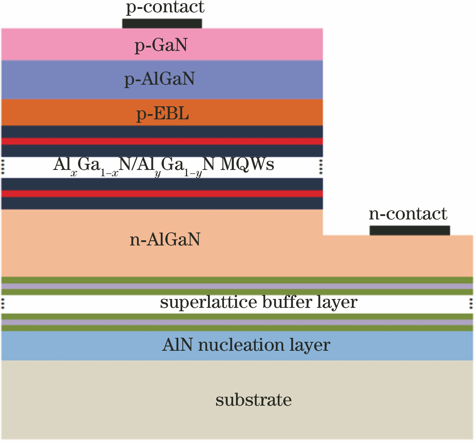
Fig. 1. Schematic of epitaxial structure for DUV LED
![Simulation results. (a) Relative dielectric constant of AlxGa1-xN layer versus AlN composition; (b) electric fields in tunneling regions for devices A1 and A2 at equilibrium (Inset shows peak field intensity versus polarization level). Reproduced from Ref. [57] with permission of Wiley](/richHtml/lop/2019/56/6/060001/img_2.jpg)
Fig. 2. Simulation results. (a) Relative dielectric constant of AlxGa1-xN layer versus AlN composition; (b) electric fields in tunneling regions for devices A1 and A2 at equilibrium (Inset shows peak field intensity versus polarization level). Reproduced from Ref. [57] with permission of Wiley
Fig. 3. Simulation results. (a) Electric field profiles in tunneling regions for devices A4, A5, and A6 at injection current of 35 mA; (b) hole concentration profiles in active region for devices A3, A4, A5, and A6 at current injection of 35 mA; (c) light output power for devices A3, A4, A5, and A6 versus injection current
Fig. 4. Lateral hole concentration profiles in last quantum well for devices A3, A4, A5, and A6 at injection current of 35 mA
Fig. 5. Current versus applied voltage for devices A3, A4, A5, and A6
Fig. 6. Energy band diagram and electric field profile in interface depletion region of p-AlxGa1-xN layer. (a) Energy band diagram; (b) schematic of electric field profile. Reproduced from Ref. [58] with permission of Optical Society of America
Fig. 7. Simulation results. (a) Electric field profiles in hole supplier layer for five groups of DUV LED devices; (b) calculated power densities for five groups of DUV LED devices at injection current of 200 A·cm-2. (a) is reproduced from Ref. [58] with permission of Optical Society of America. (b) is reproduced from Ref. [4], and the value is summarized according to the report in Ref. [58]
Fig. 8. I-V characteristic comparison. (a) Original device and Reference device; (b) Reference device and device B1; (c) Reference device, device B2 and device B3. Reproduced from Ref. [58] with permission of Optical Society of America
Fig. 9. Schematic and simulation results. Schematic of energy bands for (a) DUV LED with the conventional p-EBL and (b) DUV LED with the p-AlxGa1-xN/AlyGa1-yN/AlxGa1-xN (x>y) EBL; (c) hole concentration profiles in p-EBL and p-AlGaN layers. Reproduced from Ref. [59] with permission of American Chemical Society
Fig. 10. Simulation and experimental results. (a) Hole concentration profiles in quantum wells for devices C1 and C2; (b) measured optical power and EQE for devices C1 and C2; (c) calculated optical power and EQE for devices C1 and C2. Reproduced from Ref. [59] with permission of American Chemical Society
Fig. 11. Simulation results at injection current of 35 mA. (a) Light output power for DUV LEDs in terms of the polarization level; (b) hole concentration profiles in quantum wells, p-AlGaN layer and p-GaN layer for devices D1, D2, D3, D4, and D5. Reproduced from Ref. [79] with permission of Elsevier
Fig. 12. Simulation results at injection current of 35 mA. (a) Light output power for DUV LED versus polarization level at p-EBL/p-AlGaN/p-GaN interface; (b) hole concentration profiles in quantum well, p-AlGaN layer and p-GaN layer for devices D6, D7, D8, and D9; (c) electric field profiles for devices D6, D7, D8, and D9. Reproduced from Ref. [79] with permission of Elsevier
Fig. 13. Carrier concentration profiles for devices E1, E2, and E3 at injection current of 100 A/cm2. (a) Electron profiles; (b) hole profiles. Reproduced from Ref. [83] with permission of Optical Society of America
Fig. 14. Energy band diagram and optical output power. (a) Schematic of energy bands for UVA LED; (b) measured (curve) and calculated (scatterplot) optical powers for devices E1,E2, and E3 in terms of current. Reproduced from Ref. [84] with permission of Optical Society of America
|
Table 1. Devices with different AlN compositions for p-EBL and the p-AlxGa1-xN layers. Reproduced from Ref. [58] with permission of Optical Society of America
|
Table 2. Work done to holes by electric field within p-AlGaN/p-GaN structure for devices D6, D7, D8, and D9 at injection current of 35 mA. Reproduced from Ref. [79] with permission of Elsevier

Set citation alerts for the article
Please enter your email address
© Copyright 2018-2021 | Chinese Laser Press. All Rights Reserved 沪ICP备15018463号-20