Author Affiliations
1College of Optoelectronic Technology, Chengdu University of Information Technology, Chengdu 610225, China2Institute of Fundamental and Frontier Sciences, University of Electronic Science and Technology of China, Chengdu 610054, China3Department of Physics and Astronomy and Nanoscale and Quantum Phenomena Institute, Ohio University, Athens, Ohio 45701, USA4School of Physics and Technology, Center for Nanoscience and Nanotechnology, Wuhan University, Wuhan 430072, China5CINBIO, Universidade de Vigo, Vigo 36310, Spain6e-mail:7e-mail:show less
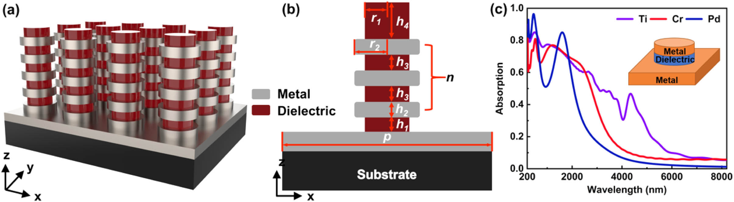
Fig. 1. Ultra-broadband plasmonic metamaterial absorber. (a) 3D schematic of the absorber. (b) Front view of the unit cell of the absorber. (c) Typical metamaterial absorber with sandwiched MDM configuration and obtained absorption spectra. The geometric parameters are consistent with model 1. The period of the structure is 220 nm, thickness of the substrate is 300 nm, radius of metal and dielectric is 100 nm, and heights of metal and dielectric are 45 and 25 nm, respectively.
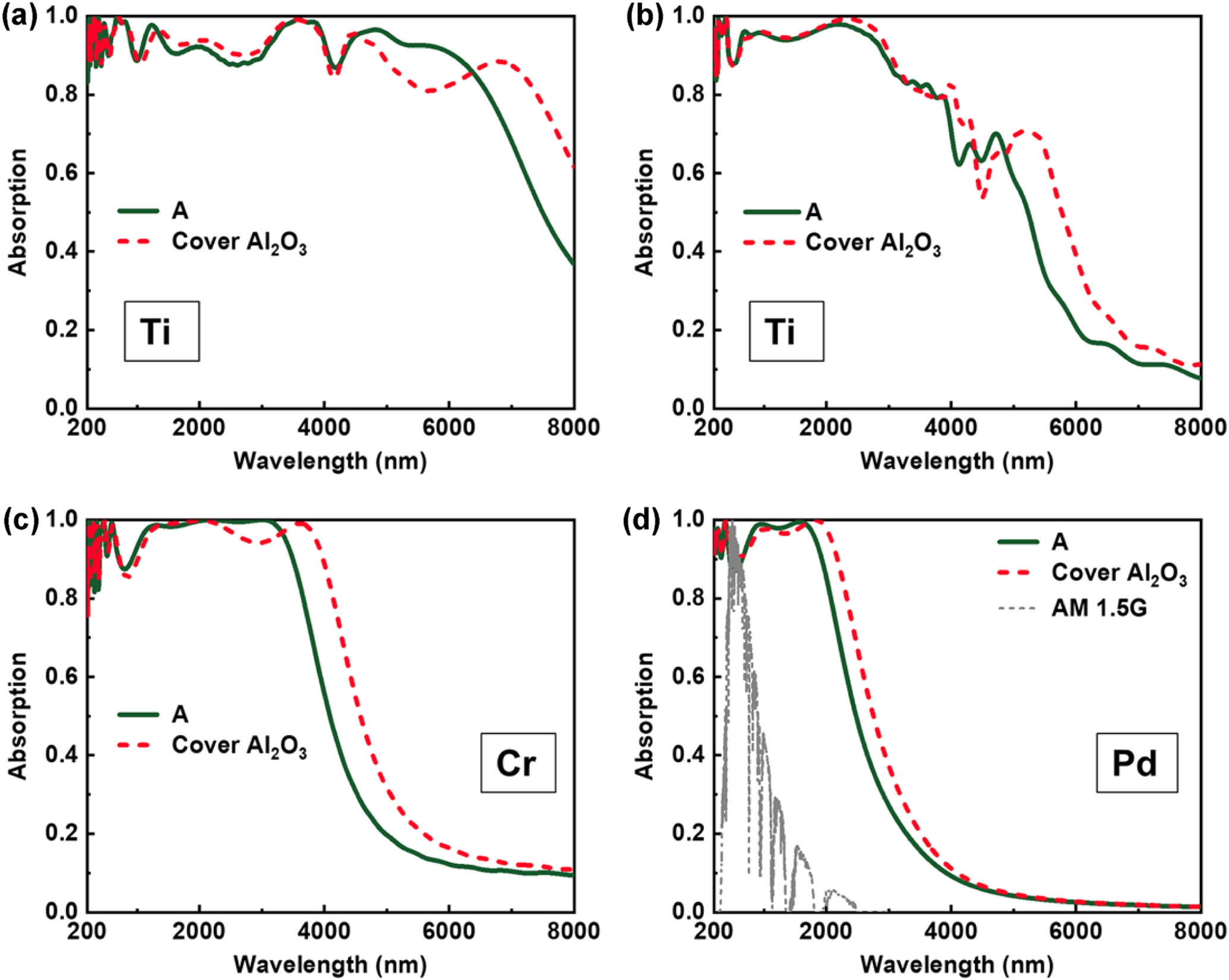
Fig. 2. Absorption spectra of the proposed absorbers. (a)–(d) Obtained absorption spectra with (red dashed line) or without (dark green solid line) covering a layer of Al2O3 of models 1 to 4. The grey dashed line indicates the standard spectrum of solar radiance AM 1.5.
Fig. 3. Absorption under different incident conditions. (a) Contour plot of the absorption spectra for TE mode and (b) TM mode at different incident angles from 0° to 70° with a step of 5°. (c) Absorbance spectra with different incident angles for TE mode and (d) TM mode. (e) Average absorption from 0.2 to 7 μm as a function of incident angle with TE and TM modes.
Fig. 4. Electric field (|E|) distributions (surface plot) and Poynting vectors (white arrows) in a unit cell at different wavelengths, where TM-polarized light with normal incidence is chosen. The upper figures represent the short-wavelength region; lowers are the long-wavelength region. The position of the monitor is located at y=0 nm. The red dashed frame indicates where the light is confined in the absorber.
Fig. 5. Absorber structure can be considered as a set of G-SPP resonators. (a) Schematic of light propagation in the cross section of the absorber and the resulting resonance mode. (b) G-SPP mode effective index with various dielectric film thicknesses and (c) its propagation lengths as a function of incident wavelengths. (d) Equivalent structure diagram of the absorber section. (e) Required height to maintain FP resonance versus resonance wavelength for different phase shifts. The red dashed line shows the corresponding height in the absorber. (f) Phase shift of the G-SPP in cavity 2. The monitor is placed in the center of the cavity.
Fig. 6. Absorption spectra with different structure parameters. (a) Period p. (b) Radius of dielectric nanowires r1. (c) Radius of dielectric nanorings r2. (d) Distance between the bottom nanoring and metallic film h1. (e) Height of the nanorings h2. (f) Number of nanorings coated on a nanowire n.
Fig. 7. Average absorption with different structure parameters. (a) Period p. (b) Radius of dielectric nanowires r1. (c) Radius of dielectric nanorings r2. (d) Distance between the bottom nanoring and metallic film h1. (e) Height of the nanorings h2. (f) Number of nanorings coated on a nanowire n.
Fig. 8. Magnetic field (|H|) distributions and Pabs (in log scale) in a unit cell at typical wavelengths, where TM-polarized light with normal incidence is chosen. The position of the monitor is located at y=0 nm.
Fig. 9. Absorption spectra with different structure parameters. (a) Distance between two nanorings h3. (b) Remaining height of dielectric nanowires h4. (c) Refractive index of the dielectric RI.
Fig. 10. Average absorption with different structure parameters. (a) Distance between two nanorings h3. (b) Remaining height of dielectric nanowires h4. (c) Refractive index of the dielectric RI.
Absorber | Metal | (nm) | (nm) | (nm) | (nm) | (nm) | (nm) | (nm) | | RI |
---|
Model 1 | Ti | 220 | 75 | 100 | 0 | 45 | 25 | 360 | 8 | 2.5 | Model 2 | Ti | 270 | 75 | 115 | 0 | 50 | 5 | 185 | 5 | 2.5 | Model 3 | Cr | 220 | 75 | 100 | 0 | 70 | 25 | 245 | 3 | 2.2 | Model 4 | Pd | 250 | 75 | 100 | 0 | 45 | 30 | 110 | 3 | 1.8 |
|
Table 1. Optimized Geometric Parameters of the Proposed Absorbers
Structure | Structure Period (μm) | Absorption Bandwidth (μm) | Average Absorption | Scalability to Large Areas | Fabricating Difficulty | Ref. |
---|
Four resonators with MDM tri-layers | 6.76 | 7.8–12.1 | 90% | No | Challenging (sim.) | Guo et al. (2016) [26] | Tapered multilayers | 4 | 0.2–15 | | No | Challenging (sim.) | Yue et al. (2020) [19] | Four resonators with MDM tri-layers | 3.72 | 6.3–14.8 | 90% | No | Medium (sim.) | Luo et al. (2020) [27] | Three resonators with MDM tri-layers | 3.6 | 4–16 | | No | Low (exp.) | Shrestha et al. (2018) [28] | Embedding the MDM cavity into dielectrics | 2.4 | 8–16 | 94% | No | Challenging (sim.) | Luo et al. (2019) [29] | Tapered multilayers | 1.6 | 1–14 | | No | Challenging (sim.) | Liang et al. (2013) [18] | MDM tri-layers | 1.6 | 8–14 | | No | Low (exp.) | Zhou et al. (2021) [30] | Gosper curve resonators with MDM tri-layers | 1.55 | 2.64–9.79 | 95.78% | No | Challenging (sim.) | Zhou et al. (2019) [16] | Five resonators with multilayers | 1.4 | 8–14 | | No | Low (sim.) | Zhou et al. (2020) [31] | Wire-grid with multilayers | 1 | 1.98–11.74 | | No | Low (exp.) | Zhong et al. (2017) [32] | Tapered multilayers | 0.8 | 2.5–7 | 86.4% | No | Challenging (sim.) | Cui et al. (2012) [33] | Nanoparticles embedded in nanopores | 0.45 | 0.4–10 | 99% | Yes | Low (exp.) | Zhou et al. (2016) [20] | This absorber | 0.22 | 0.2–7 | | Yes | Medium (sim.) | This work |
|
Table 2. Comparison of Representative Works on Broadband Absorbers Operating at Least to Mid-Infrared Wavelengtha
Figure | (nm) | (nm) | (nm) | (nm) | (nm) | (nm) | (nm) | | RI |
---|
Fig. 6(a) | Varied | 75 | 100 | 0 | 45 | 25 | 360 | 8 | 2.5 | Fig. 6(b) | 220 | Varied | 100 | 0 | 45 | 25 | 360 | 8 | 2.5 | Fig. 6(c) | 220 | 75 | Varied | 0 | 45 | 25 | 360 | 8 | 2.5 | Fig. 6(d) | 220 | 75 | 100 | Varied | 45 | 25 | 360 | 8 | 2.5 | Fig. 6(e) | 220 | 75 | 100 | 0 | Varied | 25 | 360 | 8 | 2.5 | Fig. 6(f) | 220 | 75 | 100 | 0 | 45 | 25 | 360 | Varied | 2.5 | Fig. 9(a) | 220 | 75 | 100 | 0 | 45 | Varied | 360 | 8 | 2.5 | Fig. 9(b) | 220 | 75 | 100 | 0 | 45 | 25 | Varied | 8 | 2.5 | Fig. 9(c) | 220 | 75 | 100 | 0 | 45 | 25 | 360 | 8 | Varied |
|
Table 3. Parameter Settings When Studying the Effect of Different Parameters on Absorption