Baoqing Wang1,2,†, Cuiping Ma2,†, Peng Yu1,6,*, Alexander O. Govorov3..., Hongxing Xu4, Wenhao Wang2, Lucas V. Besteiro5, Zhimin Jing2, Peihang Li2 and Zhiming Wang2,7,*|Show fewer author(s)
Broadband absorbers generally consist of plasmonic cavities coupled to metallic resonators separated by a dielectric film, and they are vertically stacking configurations. In this work, we propose an ultra-broadband nanowire metamaterial absorber composed of an array of vertically aligned dielectric nanowires with coaxial metallic rings. The absorber shows strong absorption from 0.2 to 7 μm with an average absorption larger than 91% due to the excitation of gap surface plasmon polariton modes in Fabry–Perot-like resonators. Moreover, a refractory dielectric cladding can be added to improve the thermal stability of the absorber, showing a negligible impact on its absorption performance. The proposed absorber may find potential applications in solar energy harvesting, infrared imaging and spectroscopy, and optoelectronic devices.
1. INTRODUCTION
Electromagnetic wave absorbers working at different wavelengths are important for numerous applications such as photochemistry, photovoltaics, solar thermophotovoltaics (STPVs), radiative cooling, and photodetection [1,2]. Metamaterials are built by artificially designed subwavelength units, demonstrating unique optical features unavailable in natural materials [1]. They have been widely used for perfect absorbers [3,4]. Metamaterial absorbers can be classified into broadband and narrowband. Broadband metamaterial absorbers can maintain high light absorption over a large bandwidth, and they are critical for applications such as photovoltaics, photodetectors, solar steam generation, and manipulation of mechanical resonances [1]. Various metastructures have been proposed for broadband light absorption, including metallic gratings [5], nanoparticles [6], photonic crystals [7], cavities [8], and carbon-based materials [9,10]. As a result, they can be used for photodetection [11], solar desalination [6], thermophotovoltaics [12], and optofluidics [13].
So far, tremendous efforts have been contributed to broadening the wavelength range of the metamaterial absorber. The most straightforward method is to couple multi-sized metallic resonators to achieve broadband absorption by covering the electromagnetic spectrum with the different resonances coupled in the systems [8,14–16]. Although the absorption bandwidth can be easily adjusted by changing the structure parameters, integrating multi-resonators in a unit cell greatly increases the size of the structure. Moreover, few of these reported structures can simultaneously achieve broadband absorption in the full range from visible to mid-infrared. Tapered metal–dielectric–metal (MDM) multilayer absorbers have great potential to achieve ultra-broadband absorption. For example, several works have demonstrated strong absorption from 0.2 to 3 μm [17], 1 to 14 μm [18], and even 0.2 to 15 μm [19]. However, their manufacturing is demanding. The multilayer stacking of different sized structures increases their periods and heights, and the hard-to-adjust spectral range further limits practical application. Embedding nanoparticles in a dielectric matrix can be applied to achieve broadband absorption [6,20]. The structure can be designed within a small period according to the size of the dielectric porousness. However, the nanoparticles suffer from thermal deformation even with a protective layer due to the agglomeration between nanoparticles in a harsh environment [11,21].
Here, we propose an ultra-broadband plasmonic metamaterial absorber based on a horizontally stacked metal–dielectric configuration with coupled metallic rings in the vertical dielectric axes. The structure’s period is only 220 nm (nearly 1/16 of the center wavelength), the total height of stacked metal nanoring is 535 nm, and the average absorption is over 91%, from 0.2 to 7 μm. To the best of our knowledge, it is the most miniature plasmonic metamaterial absorber reported for ultra-broadband absorption. Significantly, the obtained absorption spectral range can be easily modified by changing the materials or structure parameters, which can cover from 0.2 to 4 μm with an average absorption , 0.2 to 3 μm with an average absorption , and 0.2 to 2 μm with an average absorption . The broadband absorption originates from the coupling of gap surface plasmon polariton (G-SPP) mode in a Fabry–Perot (FP)-like resonator. Moreover, the absorber’s thermal stability can be improved by adding a cladding layer of a refractory dielectric with negligible impact on the absorption performance; the absorber’s performance shows robustness against large changes of both incident and polarization angles. The designed absorber can be fabricated in a large area using coaxial lithography technology [22,23]. This allows for practical applications that require large areas, including energy harvesting, STPVs, and solar steam generation.
Sign up for Photonics Research TOC. Get the latest issue of Photonics Research delivered right to you!Sign up now
2. THEORETICAL MODEL
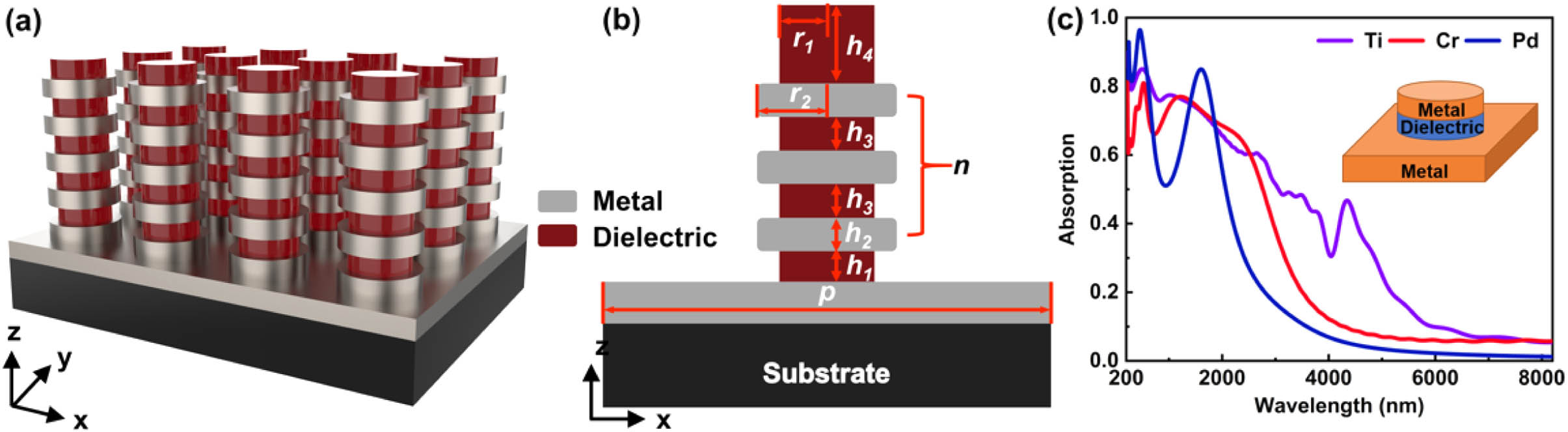
Figure 1.Ultra-broadband plasmonic metamaterial absorber. (a) 3D schematic of the absorber. (b) Front view of the unit cell of the absorber. (c) Typical metamaterial absorber with sandwiched MDM configuration and obtained absorption spectra. The geometric parameters are consistent with model 1. The period of the structure is 220 nm, thickness of the substrate is 300 nm, radius of metal and dielectric is 100 nm, and heights of metal and dielectric are 45 and 25 nm, respectively.
The numerical simulations are performed using commercial software Lumerical finite-difference time-domain (FDTD) solutions and COMSOL Multiphysics. Periodic boundary conditions are applied for the and directions, and a plane wave source is placed at 5 μm above the structure. To guarantee the accuracy of simulation results, we optimized mesh accuracy and perfectly matched layer (PML) boundary conditions until the results are convergent. A mesh override region of is used for the whole structure, and the mesh accuracy level is set to six in FDTD solutions. PMLs with 64 layers are used along the direction to eliminate boundary scattering. The absorption () is calculated using the equation , where and refer to transmission and reflection (here ), respectively. The material properties of Ti, Cr, and Pd are taken from Ref. [24]. The refractive index of is taken from Ref. [25].
3. RESULTS AND DISCUSSION
A. Absorption Performance
Figure 2.Absorption spectra of the proposed absorbers. (a)–(d) Obtained absorption spectra with (red dashed line) or without (dark green solid line) covering a layer of of models 1 to 4. The grey dashed line indicates the standard spectrum of solar radiance AM 1.5.
Furthermore, facile structures with different materials are designed to reduce manufacturing difficulty and obtain selective absorption in various electromagnetic wavelength bands. In model 3, we use Cr to substitute Ti, and each nanowire is coated with only three nanorings. In the wavelength ranging from 0.2 to 3 μm, the average absorbance is significantly enhanced, reaching 97% [Fig. 2(c)]. Yet, the absorption efficiency decreases sharply from 3 to 7 μm. For the application of STPV, the absorber should simultaneously satisfy the stringent requirements of wavelength-selective and low thermal radiation loss [9]. Here, we chose Pd for the selective absorption, and the structure parameters are shown in model 4. In the wavelength ranging from 0.2 to 2 μm, the average absorption is about 96%, while it drops to 10% from 2.5 to 7 μm. This design can significantly improve solar energy collection efficiency, reduce thermal radiation loss, and improve the performance of STPV. Thus, the proposed absorbers suggest promising broad applicability in STPVs.
A vital characteristic of a technologically viable absorber is its absorption performance in harsh conditions. Plasmonic nanostructures exposed to high temperatures often cause thermally induced deformation or chemical instability. Experiments have shown that covering a layer of 4 nm on the surface of the device does not affect its performance and can significantly improve its chemical and thermal stability [34]. Based on this strategy, we studied the absorbers’ performance after covering a layer of 5 nm on its surface. Figure 2 (red dashed line) shows that the absorption changes slightly after covering an layer. However, the overall absorption efficiency has been improved, suggesting promising perspectives in the applications of photovoltaics and STPVs.
To further characterize the optical performance of the proposed broadband absorber, we simulated the absorption under different incident conditions. Figure 3 shows the obtained absorption spectra of model 1 with varying incident angles under the incidence of transverse electric (TE) and transverse magnetic (TM) polarized light. The incident angle is changed from 0° to 70° in a step of 5°, as shown in Figs. 3(a) and 3(b), and the average absorption from 0.2 to 7 μm as a function of incident angle is also calculated, as shown in Fig. 3(e). For the TE mode, an average absorption of 90% in the wavelength range of 0.2 to 7 μm is nearly unchanged when is up to 45°. As the incident angle increases, the absorption spectrum becomes less flat, and bands with appreciably less absorbance appear due to the weak coupling of the incident electromagnetic field. In contrast, the average absorption remains at , with incident angles up to 70°. For the TM mode, the absorption efficiency is slightly higher than for the TE mode with incident angles up to 60° due to the increased coupling of surface plasmons (SPs). Compared with the TE mode, after the incident angle is greater than 60°, the absorption efficiency decreases significantly. However, the average absorption is still larger than 75%. Therefore, these results indicate that our ultra-broadband plasmonic absorber has wide-angle and polarization-insensitive characteristics in the visible to mid-infrared region.
Figure 3.Absorption under different incident conditions. (a) Contour plot of the absorption spectra for TE mode and (b) TM mode at different incident angles from 0° to 70° with a step of 5°. (c) Absorbance spectra with different incident angles for TE mode and (d) TM mode. (e) Average absorption from 0.2 to 7 μm as a function of incident angle with TE and TM modes.
To reveal the broadband absorption mechanism of the proposed metamaterial absorber, we simulated the electric field (), magnetic field (), and power of absorbed light () distributions in the plane. As shown in Fig. 4, the electric field distributions are confined mainly in the metal–dielectric interface and the gap between two adjacent nanorings. Since a single metal–dielectric interface can generate individual SPPs, placing two (or more) metal–dielectric interfaces close to each other introduces the coupled SPP mode, called G-SPP [35,36]. This G-SPP mode can slow down the previous SPP mode, and make nano-sized field localization at any wavelength accessible. Therefore, the absorber can be considered as the combination of several symmetric MDM structures.
Figure 4.Electric field () distributions (surface plot) and Poynting vectors (white arrows) in a unit cell at different wavelengths, where TM-polarized light with normal incidence is chosen. The upper figures represent the short-wavelength region; lowers are the long-wavelength region. The position of the monitor is located at . The red dashed frame indicates where the light is confined in the absorber.
The Poynting vectors shown as a white arrow in Fig. 4 are used to complement the above analysis and reveal the details of light propagation in metamaterials. The Poynting vectors above the pillar travel downward through the top of the system, nearly unaffected by the nanorings until they curl at the bottom. At such a position, the Poynting vectors are reflected into the resonator by the substrate. In the case of this multilayer structure, the resonance of the upper layer is excited once more by the reflected wave from the lower layer. The same pattern can also be found in the magnetic field distribution (Appendix A). Thus, this absorber can generate a multiplied effect to confine light, which results in the electric field intensity of the upper nanoring being much higher than that of the lower layer. Then the light is confined in a certain position inside the absorber, as shown in the red dashed frame in Fig. 4. The inside of the nanowire can be regarded as an FP-like resonance cavity. Constructive interference in the propagating G-SPP causes the standing-wave resonance in this cavity for certain wavelengths, leading the remaining energy to be dissipated in the nanoring here.
To understand how incident light is trapped in the structure and verify the rationality of the hypotheses above, a model with a simplified structure and an effective index method is used for quantitative investigation of the absorber’s performance. Through the analysis above, the absorber can be considered as the combination of several symmetrical MDM configurations, as shown in Fig. 5(a). This simplified model clearly shows the light propagation process in the absorber, in which the coupling of G-SPP modes in FP-like resonators leads to absorption enhancement. The G-SPP existing in this MDM structure can be considered as a wave propagating in a uniform medium with a mode effective index [35] . Here, is the free-space wave vector, and is the G-SPP propagation constant. The G-SPP propagation constant is calculated by the following expression [35]: where , , and is the gap between two metal nanorings. Figure 5(b) shows the value of the mode effective index with various thicknesses of the dielectric layer . The mode index is larger than the dielectric refractive index [navy dashed line in Fig. 5(b)] in most of the wavelength range, which indicates that the structure can confine the SPP well. The propagation length of G-SPP, , as a function of resonance wavelength , is also calculated, as shown in Fig. 5(c). The long propagation length indicates better confinement on the G-SPP [37]. Changing the thickness of the dielectric layer has negligible impact on the mode index and propagation length. This indicates that affects absorber performance slightly, which is consistent with the result shown in Appendix B and Appendix C. Thus, the obtained results confirm that realization of the G-SPP waveguide featuring subwavelength confinement in the absorber is accessible.
Figure 5.Absorber structure can be considered as a set of G-SPP resonators. (a) Schematic of light propagation in the cross section of the absorber and the resulting resonance mode. (b) G-SPP mode effective index with various dielectric film thicknesses and (c) its propagation lengths as a function of incident wavelengths. (d) Equivalent structure diagram of the absorber section. (e) Required height to maintain FP resonance versus resonance wavelength for different phase shifts. The red dashed line shows the corresponding height in the absorber. (f) Phase shift of the G-SPP in cavity 2. The monitor is placed in the center of the cavity.
When the G-SPP reaches the end of nanorings along the axis, it will be effectively reflected due to the large mode index. Constructive interference inside the nanorings results in FP-like cavity resonance, leading to larger field enhancement. The equivalent structure diagram of the absorber is shown in Fig. 5(d). FP resonance is generated mainly inside cavity 1 and occurs only when the following equation is satisfied [35]: where is the height of the resonator, is the mode index of the equivalent structure, and is the reflection phase, which changes from zero to . We do not know exactly the value of . However, according to Eq. (2), the needed height of the cavity to generate FP resonance can be predicted at a certain resonance wavelength under a fixed phase. Since the absorber can generate a multiplied effect, the height can be doubled in this structure, which is consistent with the calculated , as shown in Fig. 5(e). When the phase shift is greater than , the calculated resonant cavity length is smaller than the designed absorber height in the long-wavelength range, which provides a theoretical basis for the high absorption of the absorber in this region. In addition, cavity 2 (black dashed frame) provides the distance through which the plasmon wave can propagate. Since the phase shift in this internal cavity is small [Fig. 5(f)], out-of-interface plasmon waves can be incident to the metal ring directly. If the period increases, the probability of the wave hitting the metal ring will decrease. The outgoing wave cannot be confined in the cavity, making the energy unable to be consumed in the metal. This conclusion is also consistent with the value given in Figs. 6(a) and 7(a).
Figure 6.Absorption spectra with different structure parameters. (a) Period . (b) Radius of dielectric nanowires . (c) Radius of dielectric nanorings . (d) Distance between the bottom nanoring and metallic film . (e) Height of the nanorings . (f) Number of nanorings coated on a nanowire .
Figure 7.Average absorption with different structure parameters. (a) Period . (b) Radius of dielectric nanowires . (c) Radius of dielectric nanorings . (d) Distance between the bottom nanoring and metallic film . (e) Height of the nanorings . (f) Number of nanorings coated on a nanowire .
The optimized performance of the absorber is obtained through an extensive parameter sweep. To further clarify the light absorption mechanism and structure fabrication tolerance, the absorption performance with various structure parameters is shown in Fig. 6 and Fig. 9 (Appendix B). The relevant parameter settings are shown in Table 3 in Appendix B. The average absorption from 0.2 to 7 μm is shown in Fig. 7. First, the impact of the period on performance is studied by keeping other geometry parameters fixed. Figure 6(a) shows that the absorption efficiency is very sensitive to the period . Higher absorption efficiency and broader absorption bandwidth are obtained in a smaller period. This is due to the increase of the gap between two adjacent vertical nanorings with the increased period, and thus G-SPPs reflected at the termination cannot be effectively confined, resulting in considerable radiation losses in cavity 2 [36,38]. Similar phenomena can be observed in Figs. 7(b) and 7(c). This is because a decrease in or an increase in ( nm) will increase the thickness of the metal ring, weakening the G-SPP and FP-like resonance coupling effect due to the reduced cavity size. On the contrary, as the thickness of the metal ring decreases, ohmic loss in the metal will further decrease, thereby lowering absorption efficiency.
Parameter Settings When Studying the Effect of Different Parameters on Absorption
Figure
(nm)
(nm)
(nm)
(nm)
(nm)
(nm)
(nm)
RI
Fig. 6(a)
Varied
75
100
0
45
25
360
8
2.5
Fig. 6(b)
220
Varied
100
0
45
25
360
8
2.5
Fig. 6(c)
220
75
Varied
0
45
25
360
8
2.5
Fig. 6(d)
220
75
100
Varied
45
25
360
8
2.5
Fig. 6(e)
220
75
100
0
Varied
25
360
8
2.5
Fig. 6(f)
220
75
100
0
45
25
360
Varied
2.5
Fig. 9(a)
220
75
100
0
45
Varied
360
8
2.5
Fig. 9(b)
220
75
100
0
45
25
Varied
8
2.5
Fig. 9(c)
220
75
100
0
45
25
360
8
Varied
In the following, the influence of height (, , , ), numbers , and refractive index RI on absorption spectra is also investigated. Figure 6(d) shows the influence of height on absorption performance. As increases, the average absorption gradually decreases, but there is still considerable absorption in the long-wavelength region. It can be understood that as increases, the confined light in the bottom cannot be well confined through this appearing aperture gap. Also, the parameters of and have similar effects on absorption performance because with the increase of or , the light trapping effect increases, resulting in a gradual increase in absorption. When the height of the metallic ring increases to a certain value, the absorption no longer increases. Due to the further increase of or , the optical propagation direction may be affected, leaving the coupling effect weakened. Thus, the average absorption is reduced. In addition, from the above analysis, it can be seen that absorption performance is very sensitive to parameters of , , and . However, the accuracy of these structure parameters can be effectively controlled through the fabrication process. For example, the height of () can be determined before fabrication; and can be well controlled through the etch process.
4. EXPERIMENTAL FEASIBILITY
Since RI has little effect on the average absorption efficiency (Appendix C), we take silicon as an example to illustrate the experiment’s feasibility. The other materials, (), (), (), etc., can also be designed as dielectric nanowires in the absorber [39]. The proposed absorber can be fabricated in a large area by the coaxial lithography method [22,23]. First, Si nanowire arrays with well-defined parameters should be prepared, which can be fabricated by a combination of colloidal lithography and metal-assisted chemical etching (MACE) [40]. Then, Si nanowire arrays covered with a shell are embedded with a polymer film, and the shell is removed to form the desired pores. Next, we alternately use electrodeposition or vacuum evaporation with different metals in the pores to obtain the desired nanocolumn. Finally, undesired polymer film and metals are removed to get the proposed absorber.
5. CONCLUSION
In summary, an ultra-small sized nanowire metamaterial absorber coupled with metallic rings in the vertical dielectric axes is proposed in this work. The absorber has the smallest size and can be fabricated in a larger area simultaneously, hence benefiting the integration and miniaturization of optical devices. This absorber can generate multiple effects to confine incident light. Due to the excitation of G-SPP modes in FP-like resonators, the absorber exhibits ultra-broadband absorption in the wavelength ranging from 0.2 to 7 μm, and the average absorption is . Especially, the obtained absorption spectral range can be easily tuned by changing the structure parameter or materials. Moreover, the absorber shows remarkable polarization and wide incident angle insensitivity. The absorber can be protected by a layer of with negligible impact on absorption performance, indicating its potential application for solar energy harvesting, radiative cooling, infrared imaging and spectroscopy, image detectors, and optoelectronic devices.
APPENDIX A
As illustrated in Fig. 8, the magnetic field is located primarily at the top of the resonator and gradually moves down to the bottom. Incident light gets trapped and gradually moves upward as the wavelength increases. Compared with the resonance wavelength of 5.5 μm, the trapped light at 8 μm is no longer localized at the interior but dispersed to the surface of the nanoring, resulting in a decrease in absorption efficiency.
Figure 8.Magnetic field () distributions and (in log scale) in a unit cell at typical wavelengths, where TM-polarized light with normal incidence is chosen. The position of the monitor is located at .
Figure 9.Absorption spectra with different structure parameters. (a) Distance between two nanorings . (b) Remaining height of dielectric nanowires . (c) Refractive index of the dielectric RI.
Figure 10.Average absorption with different structure parameters. (a) Distance between two nanorings . (b) Remaining height of dielectric nanowires . (c) Refractive index of the dielectric RI.
To reveal the energy dissipation process, we calculated the absorbed electromagnetic power using the equation, , where is the angular frequency, is the imaginary part of the permittivity, and is the amplitude of the total electric field. The optical absorption process can be divided into light harvesting, light confinement, and energy dissipation. The light-harvesting process can be achieved by adjusting the structural parameters to achieve impedance matching. In the short-wavelength region, the trapped light can propagate along with the metal–dielectric interface and exciting SP resonance. In this region, most of the light energy is dissipated in the nanorings to generate heat through intrinsic ohmic loss, and then the remaining power is absorbed by the substrate. In addition, the undissipated energy backpropagates to the nanorings, which are further consumed by the SP resonance and FP cavity resonance. Thus, the synergy of these phenomena significantly increases the light confinement effect in the proposed absorber.
APPENDIX B
Absorption performance under different parameter settings is investigated. The control variable method is used here. As can be seen from these maps, our structure consistently maintains high absorption performance, which illustrates the insensitivity of the system to parameter changes. To a certain extent, our design can reduce the difficulty of sample preparation.
APPENDIX C
The effect of different parameters on the average absorption is investigated and shown in Fig. 10. High average absorption can be maintained even under wide variations of these parameters.