• Photonics Research
  • Vol. 6, Issue 12, 1151 (2018)
Yiwen Sun1, Riccardo Degl’Innocenti2, David A. Ritchie2, Harvey E. Beere2, Long Xiao2、3, Michael Ruggiero4, J. Axel Zeitler5, Rayko I. Stantchev6, Danni Chen7, Zhengchun Peng7, Emma MacPherson6、8, and Xudong Liu1、*
Author Affiliations
  • 1National-Regional Key Technology Engineering Laboratory for Medical Ultrasound, Guangdong Key Laboratory for Biomedical Measurements and Ultrasound Imaging, Department of Biomedical Engineering, School of Medicine, Shenzhen University, Shenzhen 518060, China
  • 2Cavendish Laboratory, University of Cambridge, J J Thomson Avenue, Cambridge CB3 0HE, UK
  • 3Department of Electrical Engineering and Computer Science, Massachusetts Institute of Technology, Cambridge, Massachusetts 02139, USA
  • 4Department of Chemistry, University of Vermont, 82 University Place, Burlington, Vermont 05405, USA
  • 5Department of Chemical Engineering and Biotechnology, University of Cambridge, Pembroke Street, Cambridge CB2 3RA, UK
  • 6Department of Electronic Engineering, The Chinese University of Hong Kong, Hong Kong, China
  • 7Key Laboratory of Ministry of Education for Optoelectronic Devices and Systems, College of Optoelectronic Engineering, Shenzhen University, Shenzhen 518060, China
  • 8Department of Physics, University of Warwick, Gibbet Hill Road, Coventry CV4 7AL, UK
  • show less
    DOI: 10.1364/PRJ.6.001151 Cite this Article Set citation alerts
    Yiwen Sun, Riccardo Degl’Innocenti, David A. Ritchie, Harvey E. Beere, Long Xiao, Michael Ruggiero, J. Axel Zeitler, Rayko I. Stantchev, Danni Chen, Zhengchun Peng, Emma MacPherson, Xudong Liu. Graphene-loaded metal wire grating for deep and broadband THz modulation in total internal reflection geometry[J]. Photonics Research, 2018, 6(12): 1151 Copy Citation Text show less
    (a) Graphene-loaded metal wire grating modulator in TIR geometry. The graphene device was deposited on a high-resistivity SiO2/Si substrate and placed on a Si prism. The conductivity of graphene was adjusted by the voltage between the ground (GND) and the metal grating. The incident THz signal was in s polarization. (b) Diagram of the metal grating loaded graphene structure in (a). The medium below the metal grating is the dense medium (n1), and above the metal grating is the less dense medium (n2). The THz signal is incident from the dense medium to the less dense medium in s polarization at an angle of θ. The period of the metal grating is P, and the gap width is g. The red dashed lines represent the integration loop of the electric field.
    Fig. 1. (a) Graphene-loaded metal wire grating modulator in TIR geometry. The graphene device was deposited on a high-resistivity SiO2/Si substrate and placed on a Si prism. The conductivity of graphene was adjusted by the voltage between the ground (GND) and the metal grating. The incident THz signal was in s polarization. (b) Diagram of the metal grating loaded graphene structure in (a). The medium below the metal grating is the dense medium (n1), and above the metal grating is the less dense medium (n2). The THz signal is incident from the dense medium to the less dense medium in s polarization at an angle of θ. The period of the metal grating is P, and the gap width is g. The red dashed lines represent the integration loop of the electric field.
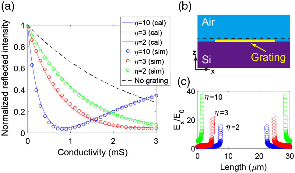
    (a) Simulation and calculation results of reflected intensity from a graphene/metal grating. The solid lines are calculation results, and the dots are simulation results with different enhancement factors (η). The black dashed lines are the calculation results without a metal grating. (b) Simulation structure of a metal grating in TIR geometry without graphene. The simulation electric field is polarized along the x direction. The black dashed line is to monitor the electric field amplitude in the simulations. (c) Simulated E-field enhancement of a THz wave with a metal grating with various grating parameters (η=2, 3, 10).
    Fig. 2. (a) Simulation and calculation results of reflected intensity from a graphene/metal grating. The solid lines are calculation results, and the dots are simulation results with different enhancement factors (η). The black dashed lines are the calculation results without a metal grating. (b) Simulation structure of a metal grating in TIR geometry without graphene. The simulation electric field is polarized along the x direction. The black dashed line is to monitor the electric field amplitude in the simulations. (c) Simulated E-field enhancement of a THz wave with a metal grating with various grating parameters (η=2, 3, 10).
    Schematic of the experimental setup and photograph of the metal grating integrated graphene device. (a) Schematic of the graphene modulator in TIR geometry. (b) and (c) are photographs of the metal grating structure. (d) Photograph of the graphene area, showing clearly the graphene covered metal grating area and bare graphene area (white dashed outline).
    Fig. 3. Schematic of the experimental setup and photograph of the metal grating integrated graphene device. (a) Schematic of the graphene modulator in TIR geometry. (b) and (c) are photographs of the metal grating structure. (d) Photograph of the graphene area, showing clearly the graphene covered metal grating area and bare graphene area (white dashed outline).
    THz peak-to-peak images of two metal gratings without graphene in TIR geometry. The peak-to-peak values are calculated from the reflected THz electric field signal from the top surface of the devices. The direction of the electric field is represented by a red double-arrow line. The slit orientation of the grating is represented by golden lines. The white dashed outlines in the images highlight the grating areas. (a), (b) Images of the 30–15 μm grating with electric field perpendicular and parallel to the silt direction. (c), (d) Images of the 30–10 μm grating with electric field perpendicular and parallel to the slit direction.
    Fig. 4. THz peak-to-peak images of two metal gratings without graphene in TIR geometry. The peak-to-peak values are calculated from the reflected THz electric field signal from the top surface of the devices. The direction of the electric field is represented by a red double-arrow line. The slit orientation of the grating is represented by golden lines. The white dashed outlines in the images highlight the grating areas. (a), (b) Images of the 30–15 μm grating with electric field perpendicular and parallel to the silt direction. (c), (d) Images of the 30–10 μm grating with electric field perpendicular and parallel to the slit direction.
    Experimental results of the metal grating integrated graphene device. (a), (b) THz peak-to-peak images of 30–15 μm and 30–10 μm grating devices without applying voltage. The graphene transferred on the metal grating is highlighted with white dashed lines. The right side of the graphene area is with a metal grating; the left side of the graphene area is without a covering metal grating. (c) and (d) are reflected waveforms by changing the gate voltages from −60 V to +60 V for 30–15 μm and 30–10 μm grating devices with (solid) and without a grating (dashed). Four insets in (c) and (d) show the peak value changes of the time-domain signal. The waveforms are shifted horizontally for clarity.
    Fig. 5. Experimental results of the metal grating integrated graphene device. (a), (b) THz peak-to-peak images of 30–15 μm and 30–10 μm grating devices without applying voltage. The graphene transferred on the metal grating is highlighted with white dashed lines. The right side of the graphene area is with a metal grating; the left side of the graphene area is without a covering metal grating. (c) and (d) are reflected waveforms by changing the gate voltages from 60  V to +60  V for 30–15 μm and 30–10 μm grating devices with (solid) and without a grating (dashed). Four insets in (c) and (d) show the peak value changes of the time-domain signal. The waveforms are shifted horizontally for clarity.
    (a) and (b) are MDs of the two devices in TIR and transmission geometries (T90). The red solid line is the MD of graphene integrated with a 30–10 μm grating; the blue solid line is the MD of graphene integrated with a 30–15 μm grating; the green dashed line is the MD of graphene without a metal grating.
    Fig. 6. (a) and (b) are MDs of the two devices in TIR and transmission geometries (T90). The red solid line is the MD of graphene integrated with a 30–10 μm grating; the blue solid line is the MD of graphene integrated with a 30–15 μm grating; the green dashed line is the MD of graphene without a metal grating.
    Yiwen Sun, Riccardo Degl’Innocenti, David A. Ritchie, Harvey E. Beere, Long Xiao, Michael Ruggiero, J. Axel Zeitler, Rayko I. Stantchev, Danni Chen, Zhengchun Peng, Emma MacPherson, Xudong Liu. Graphene-loaded metal wire grating for deep and broadband THz modulation in total internal reflection geometry[J]. Photonics Research, 2018, 6(12): 1151
    Download Citation