
Hironaru Murakami, Tomoya Takarada, Masayoshi Tonouchi. Low-temperature GaAs-based plasmonic photoconductive terahertz detector with Au nano-islands[J]. Photonics Research, 2020, 8(9): 1448
- Photonics Research
- Vol. 8, Issue 9, 1448 (2020)
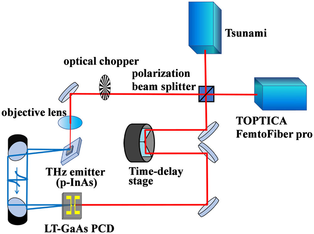
Fig. 1. Schematic illustration of THz time-domain spectroscopy (THz-TDS) system to evaluate the fabricated PCDs by using different fs-lasers with wavelengths of 800 nm and 1560 nm.
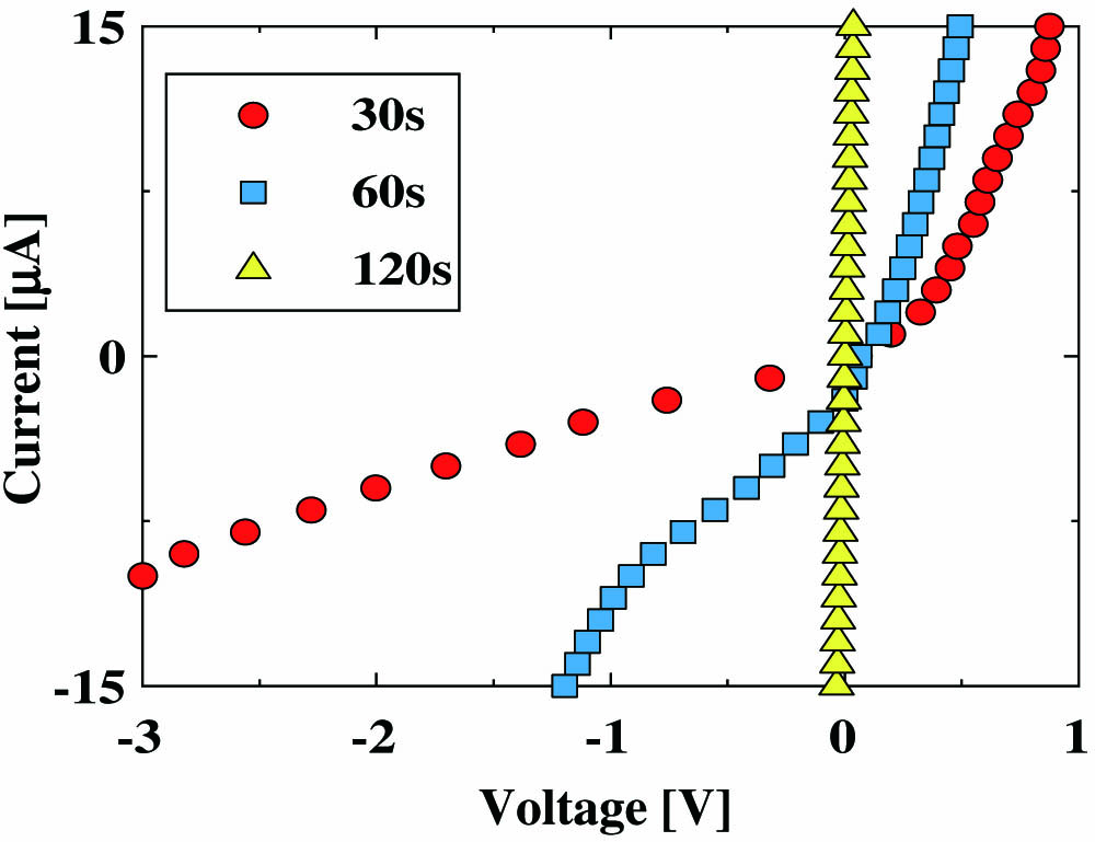
Fig. 2. Representative I -V characteristics of Si wafer deposited with gold ultrathin film. RF sputtering of gold was carried out for 30, 60, and 120 s at an RF power of 20 W.
Fig. 3. Optical microscope image of basic LT-GaAs PCD utilized in the present study. It has the structural parameters of antenna length L = 28 μm l = 4 μm w = 10 μm
Fig. 4. AFM images of the dipole gap region of LT-GaAs PCDs. Here (a) PCD-N, (b) PCD-A, and (c) PCD-B correspond to the PCD with RF sputtering time of gold for 0, 30, and 60 s, respectively.
Fig. 5. Ratios of increasing current I A / I N I B / I N I -V characteristics at 800 nm fs-laser irradiation onto the dipole gap region of PCD at a power of 10 mW.
Fig. 6. THz time-domain waveforms detected by (a) PCD-A and (b) PCD-B compared with that of PCD-N at 800 nm fs-laser excitation. Here THz pulse was emitted from the p-InAs excited by 800 nm fs-laser.
Fig. 7. Ratios of increasing current I B / I N I -V characteristics under 800 nm and 1560 nm fs-laser excitations. In the measurements fs-lasers were illuminated onto the dipole gap regions of PCD-B at a power of 10 mW for 800 nm fs-laser and 30 mW for 1560 nm fs-laser.
Fig. 8. THz time-domain waveforms detected by PCD-B and PCD-N at 1560 nm fs-laser excitation. Here THz pulse was emitted from the p-InAs excited by a 1560 nm fs-laser.
Fig. 9. FFT spectra of THz time-domain waveforms detected by PCD-B at (a) 800 nm and (b) 1560 nm fs-laser excitation corresponding to the waveforms in Fig. 6(b) and Fig. 8 , respectively. The inserted spectra in the bottom figures show those observed by PCD-N.
Fig. 10. Power dependence of I B I N
Fig. 11. Schematic illustration of excitations of electrons in Au nano-islands to the GaAs conduction band by induced electric field modulation between Au nano-islands by LSPR and change in Fermi level with electron transfer at DC bias V = 0
Fig. 12. Relationship between resonance wavelength λ L R
Fig. 13. Rectangular fitting to gold nanoparticles for aspect ratio estimation.

Set citation alerts for the article
Please enter your email address
© Copyright 2018-2021 | Chinese Laser Press. All Rights Reserved 沪ICP备15018463号-20