Abstract
We have fabricated low-temperature grown GaAs (LT-GaAs)-based plasmonic photoconductive antennas by RF sputtering of Au nanoparticles and have evaluated their terahertz detection properties. Localized surface plasmon resonance enhances the electric fields near the surface and increases the optical absorption of nanoparticles. The resonance frequency depends on the density of electrons, the effective electron mass, and the size and shape of the nanoparticles. Therefore, we tried to develop a high-sensitivity LT-GaAs photoconductive detector (PCD), which is effective over a wide range of wavelengths, by RF sputtering of Au nano-islands with a variety of aspect ratios from 1.2 to 5.1 on the dipole gap region of the PCD. As a result, we succeeded in increasing the sensitivity by 29% and 40% in the amplitude of observed terahertz pulse for 800 nm and 1560 nm femtosecond laser excitations, respectively.1. INTRODUCTION
Terahertz time-domain spectroscopy (THz-TDS) is one of the powerful tools to evaluate a variety of samples in noninvasive or label-free fashion [1–7]. Since a fiber-coupled femtosecond pulsed laser (fs-laser) with its center wavelength of 1560 nm, is robust, stable, compact, and low cost [8,9], it is considered the most useful optical source for further developments of THz technology. Therefore, THz emitters and detectors that can be operated at 1560 nm fs-laser excitation are required to utilize the fiber-coupled fs-laser as an optical source.
There are several kinds of THz emitters using the physical phenomena based on such as nonlinear frequency conversion of fs-lasers, ultrafast carrier dynamics in semiconductors, and the photo-Dember effect [10–15]. On the other hand, there are two typical methods to detect THz pulses, such as a photoconductive detector (PCD) using the photoexcited carriers generated by fs-laser irradiation and an electro-optical detector using the change in the refractive index of the electro-optic crystal due to the incident THz electric field. As for the PCD, low-temperature (200–300°C) grown GaAs (LT-GaAs) PCD is most widely used in THz application systems and is effectively used as a THz emitter and THz detector at 800 nm fs-laser excitation because of its unique properties, such as the ultrashort carrier lifetime (), large resistivity (), and relatively high carrier mobility [] [16–19].
Furthermore, LT-GaAs grown at a temperature lower than 300°C (instead of the usual 600°C) has a high density of As-antisite defects, forming deep donors’ states (mid-gap states) with energies close to mid-gap level (about 0.75 eV below the conduction band) [20]. Therefore, direct photoexcitation using a 1560 nm laser is also possible, but the photoexcitation efficiency by 1560 nm fs-laser excitation is only about 10% compared with that of 800 nm fs-laser excitation [8]. For this reason, the wavelength conversion method using a second-harmonic generation (SHG) in a nonlinear optical crystal is generally utilized as one of the simple methods to improve efficiency. However, for the conversion efficiency in SHG due to second-order nonlinear optical effects, the power density of the laser incident into an SHG crystal must be very high to obtain high conversion efficiency of 40%–50%. For example, in the case of beta-barium borate (BBO) crystals, a power density of is required to achieve a conversion efficiency of 47% [21]. In our laboratory, we also perform wavelength conversion using a BBO crystal, but the power conversion efficiency to 780 nm is only 10% even if a 1560 nm fs-laser with a power of 100 mW is incident into the BBO crystal at a narrowed focus of about 5 μm diameter (corresponding to a power density of ).
Sign up for Photonics Research TOC. Get the latest issue of Photonics Research delivered right to you!Sign up now
Therefore, many efforts are underway to improve the THz detection (and THz radiation) efficiency at 1560 nm excitation. As one of the approaches, the use of InGaAs PCD, which has a small bandgap and can be directly excited at 1560 nm, has been tried. However, there is a problem that its detection sensitivity is not so high due to its low resistance and high dark current [22,23]. Apart from the excitation wavelength, as another approach, we have optimized the antenna geometry of the dipole PCD to improve the terahertz detection sensitivity [24]. In that study, we fabricated PCDs with wide dipole electrodes to suppress the shielding of the electric field by photoexcited electron–hole pairs and to increase the reception efficiency of THz waves. As a result, we have succeeded in increasing the detection sensitivity by about 220% and increasing the dynamic range from 56 to 66 dB by using a PCD with wide dipole electrodes of 500 μm width, without reducing the observable THz bandwidth.
On the other hand, recent advances in nanofabrication technologies have led to the rapid development of plasmonic detectors based on metal nanostructures [25–39]. These devices utilize the phenomenon of localized surface plasmon resonance (LSPR), the resonance frequency of which depends on the density of electrons, the effective electron mass, and the size and shape of nanostructures [38], enabling the creation of highly efficient detectors that are specific to the optical wavelengths used. Therefore, a number of excellent detection properties have been reported. For example, Jooshesh et al. have fabricated a plasmonic PCD that has slit array plasmonic structure with 100 nm gaps and 490 nm periodicity between the dipole gap region, and they have succeeded in improving the detection sensitivity by a factor of 10 at 1560 nm excitation [25]. Therefore, if very high detection efficiency at a specific excitation wavelength is required, we should create plasmonic PCDs with precisely designed nanostructures.
However, the preparation of these nanostructured plasmonic PCDs requires a high-precision electron beam lithography system with nano-resolution, a focused ion beam (FIB) system, etc., which are often not available in a typical laboratory in university.
Therefore, in this paper we propose a plasmonic PCD that is not so highly sensitive but can be easily fabricated. Specifically, we deposited gold nanoparticles by RF sputtering between the electrodes of LT-GaAs-based PCDs and investigated the plasmonic effect at 800 nm and 1560 nm fs-laser excitations. In addition, the detectable bandwidth is also important for THz applications. Therefore, we have also checked the bandwidth associated with gold nanoparticle deposition. These results are reported here.
2. EXPERIMENTS
A. Optical System Setup
Figure 1 shows a schematic diagram of a THz time-domain spectroscopy (THz-TDS) system to evaluate the fabricated LT-GaAs PCDs of a dipole antenna structure. In this system, both fs-lasers with wavelengths of (TOPTICA FemtoFiber pro: maximum output power 400 mW, pulse width 110 fs, repetition rate 80 MHz) and (Tsunami: maximum output power 500 mW, pulse width 30 fs, repetition rate 80 MHz) are equipped as optical sources. The laser beam emitted from the fs-laser source is divided into pump and probe pulse beams by a polarization beam splitter for generating and detecting THz waves, respectively. The pump beam is modulated at a frequency of 2 kHz by using an optical chopper and irradiated to the THz emitter of a p-InAs wafer at an incident angle of 45 degrees through an objective lens, where THz wave pulses are generated by the photo-Dember effect. The generated THz waves are focused onto the PCD via two off-axis parabolic mirrors, the photoexcited carriers by probe pulses are accelerated by the electric field of the THz pulses, and then the generated photocurrent is detected by a lock-in amplifier. The THz-TDS measurement was carried out in the atmosphere at the pump and probe laser irradiation power conditions of 80 mW and 10 mW for 800 nm fs-laser excitation and 100 mW and 30 mW for 1560 nm fs-laser exciation, respectively.
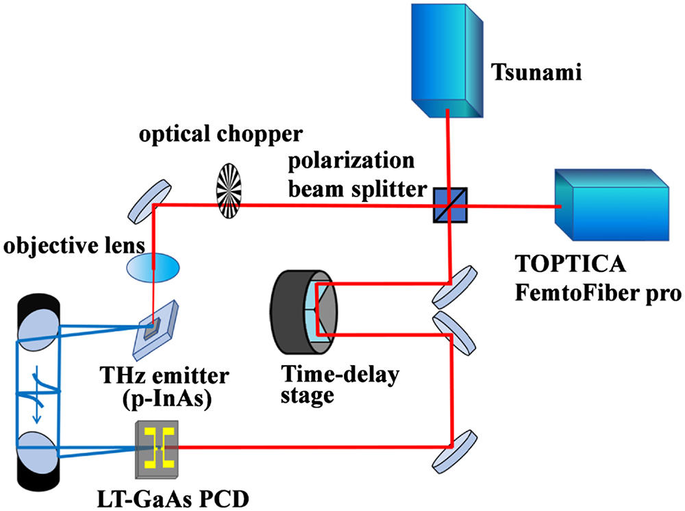
Figure 1.Schematic illustration of THz time-domain spectroscopy (THz-TDS) system to evaluate the fabricated PCDs by using different fs-lasers with wavelengths of 800 nm and 1560 nm.
B. Preparation of LT-GaAs PCD with Au Nano-Islands
In this study we tried to fabricate a plasmonic antenna by forming Au nano-islands in the dipole gap region between the electrodes of LT-GaAs PCD. Before fabrication, Au ultrathin film deposition had been examined by using Si substrates under different RF sputtering conditions, and its electrical characteristics were evaluated. As a result, it turned out that an RF power condition of 20 W is optimal for Au ultrathin film deposition using our RF sputtering system. Figure 2 shows the representative dependence of current–voltage (I-V) characteristics of the deposited Au ultrathin film at different RF sputtering time conditions (RF power: 20 W; deposition time: 30, 60, and 120 s). It can be seen that the boundary condition between island structures and continuous film states of deposited Au ultrathin film exists around the deposition time of 60 s.

Figure 2.Representative I-V characteristics of Si wafer deposited with gold ultrathin film. RF sputtering of gold was carried out for 30, 60, and 120 s at an RF power of 20 W.
On the other hand, we fabricated PCDs of dipole antenna structure on LT-GaAs, which is commercially supplied by BATOP GmbH, as follows. First, AuSn (Au: 90%, Sn: 10%) was deposited on the LT-GaAs at a thickness of 100 nm by thermal evaporation using a joule heated tungsten boat. After the deposition, the LT-GaAs/AuSn sample was in situ heated by the radiation from a joule heated tungsten boat for 60 s in a vacuum chamber, because the existence of the resistance due to the Schottky barrier at the interface of LT-GaAs/AuSn inhibits the photocurrent from flowing into the electrode. Therefore, it is not preferable for observation of THz time-domain signals and plasmonic enhancement effects [5]. Finally, it was patterned into a dipole antenna structure with a gap distance of 6 μm using electron beam lithography. Figure 3 shows a microscope image of the fabricated PCD. It has the other structural parameters of antenna length , width of the transmission line , and width of the dipole electrode . Finally, we have deposited Au ultrathin film on the dipole gap region of PCD (corresponding to the inside of the dashed circle in Fig. 3) by RF sputtering.
Figure 3.Optical microscope image of basic LT-GaAs PCD utilized in the present study. It has the structural parameters of antenna length , width of the transmission line , and width of dipole electrode .
3. EXPERIMENTAL RESULTS AND DISCUSSION
Figure 4 shows the surface morphologies of the dipole gap regions of LT-GaAs PCDs with and without Au ultrathin film observed by atomic force microscope (AFM). Here PCD-N, PCD-A, and PCD-B correspond to the PCD with RF sputtering time of Au for 0, 30, and 60 s, respectively. On the surface of PCD-N, streak-like polishing traces that are thought to be generated during the polishing process are seen. On the other hand, egg-shaped nanoparticles with a size of about 50–200 nm are seen on the surface of PCD-A, while long nano-islands with a length of about 100 to 500 nm and a width of about 100 nm are seen on the surface of PCD-B.
Figure 4.AFM images of the dipole gap region of LT-GaAs PCDs. Here (a) PCD-N, (b) PCD-A, and (c) PCD-B correspond to the PCD with RF sputtering time of gold for 0, 30, and 60 s, respectively.
First, the resistance between the electrodes in the dipole gap region was measured under a bias voltage of 1 V. As a result, it was found that the resistances of PCD-N, PCD-A, and PCD-B were 82.4, 84.5, and 77.8 MΩ, respectively, and it was confirmed that the Au particles did not cause short circuit between the electrodes. On the other hand, the resistance of a PCD after RF sputtering of Au for 90 s was also measured, but it was useless with a resistance of less than 1 MΩ.
Using the PCD-N, PCD-A, and PCD-B, the photo-induced increasing current caused by fs-laser irradiation onto the dipole gap region was observed in the I-V measurement of each PCD. Here, for the sake of simplicity, the increasing currents by fs-laser irradiation in the I-V measurements of PCD-A, PCD-B, and PCD-N are defined as , , and , respectively. Figure 5 shows the ratios of increasing current and . In the measurements, a fs-laser with a wavelength of 800 nm was irradiated onto the dipole gap regions of PCDs at a power of 10 mW. It can be seen here that a remarkable increase in the ratio is observed only for PCD-B. Further, the ratio gradually decreases with the increasing bias voltage. The difference between the characteristics of PCD-A and PCD-B is also reflected in the sensitivity of THz detection. Figure 6 shows the THz time-domain waveforms detected by PCD-A and PCD-B at 800 nm fs-laser excitation. These observations were carried out under the pump and probe laser irradiation power conditions of 30 mW and 10 mW, respectively. It can be seen that a 29% increase in the amplitude compared with that of PCD-N is achieved for PCD-B at 800 nm fs-laser excitations, while it is 12% for PCD-A.
Figure 5.Ratios of increasing current and observed in the I-V characteristics at 800 nm fs-laser irradiation onto the dipole gap region of PCD at a power of 10 mW.
Figure 6.THz time-domain waveforms detected by (a) PCD-A and (b) PCD-B compared with that of PCD-N at 800 nm fs-laser excitation. Here THz pulse was emitted from the p-InAs excited by 800 nm fs-laser.
Based on these results, we compared the ratio and the THz detection sensitivity of PCD-B at 1560 nm fs-laser excitation with those at 800 nm fs-laser excitation. Figure 7 shows the ratios of increasing current at 800 nm and 1560 nm fs-laser excitations. In the measurements, fs-lasers were irradiated onto the dipole gap regions of PCD-B at a power of 10 mW for an 800 nm fs-laser and 30 mW for a 1560 nm fs-laser. It can be seen that the ratio at 1560 nm fs-laser excitation is much larger than that at 800 nm. In the case of 800 nm fs-laser excitation, since electrons can be directly excited from the valence band to the conduction band regardless of the LSPR, the increasing current may not be significantly increased by the presence of Au nano-islands. On the other hand, the ratio at 1560 nm fs-laser excitation shows the large values in a low bias region and a gradual decrease with the increasing bias voltage. We will discuss the possibility of this phenomenon occurring later.
Figure 7.Ratios of increasing current in the I-V characteristics under 800 nm and 1560 nm fs-laser excitations. In the measurements fs-lasers were illuminated onto the dipole gap regions of PCD-B at a power of 10 mW for 800 nm fs-laser and 30 mW for 1560 nm fs-laser.
As shown above, it is noteworthy that the Au nano-islands thus formed in the dipole gap region of PCD should be useful to increase photoexcitation carriers by LSPR and shows a possibility to improve the THz wave detection efficiency at both 800 nm and 1560 nm fs-laser excitations. In fact, Fig. 8 shows the THz time-domain waveforms detected by PCD-N and PCD-B at 1560 nm fs-laser excitation. These observations were carried out under the pump and probe laser irradiation power conditions of 100 mW and 30 mW, respectively. We can see that a 40% increase in the amplitude compared with that of PCD-N is achieved at 1560 nm fs-laser excitations and that the degree of increase is larger than that observed at 800 nm fs-laser excitation as shown in Fig. 6(b). If there was not any effect by the LSPR, the photocurrent would decrease, and the terahertz detection sensitivity would also decrease because the dipole gap region of the PCD is partly covered with Au nano-islands with negative real part dielectric values at these wavelengths, i.e., the effective irradiation area of the fs-laser should be reduced. Nevertheless, the experimental increases in photo-induced current and the improvements in THz detection sensitivity show that the deposited Au nano-islands effectively work to increase the absorption of the fs-laser and to improve THz detection sensitivity by LSPR effects.
Figure 8.THz time-domain waveforms detected by PCD-B and PCD-N at 1560 nm fs-laser excitation. Here THz pulse was emitted from the p-InAs excited by a 1560 nm fs-laser.
On the other hand, Fig. 9 shows the fast Fourier transformation (FFT) spectra of the THz time-domain waveforms in Figs. 6(b) and 8. The FFT spectra show that the detectable THz bandwidth does not change, but the amplitude of spectrum increases by about 33% and 42% at 800 nm and 1560 nm fs-laser excitation, respectively. The dynamic range was 49 dB and 30 dB for 800 nm and 1560 nm fs-laser excitation, respectively. The dipole structure of PCD patterned in this study is not the most suitable structure to detect terahertz radiation with high sensitivity, particularly for 1560 nm excitation. The structure of the dipole antenna PCD has not been optimized, as this experiment was conducted only to see the plasmonic effect of gold nanoparticles. In the future, the use of wide dipole electrodes and further focused laser beams will considerably improve the dynamic range [24]. On the other hand, although the deposition of gold nanoparticles did not change the observed bandwidth, the FFT spectra show that the THz bandwidth for 1560 nm fs-laser excitation is much narrower at about 2.5 THz. In the present study, we used a cube type beam splitter to operate the 800 nm and 1560 nm lasers in the optical system, so there is a possibility that the pulse broadening of fs-lasers occurred in the BS.
Figure 9.FFT spectra of THz time-domain waveforms detected by PCD-B at (a) 800 nm and (b) 1560 nm fs-laser excitation corresponding to the waveforms in Fig. 6(b) and Fig. 8, respectively. The inserted spectra in the bottom figures show those observed by PCD-N.
In order to discuss the effect of LSPR in more detail, Fig. 10 shows the power dependence of and at 1560 nm fs-laser excitation. It can be seen that both the photo-induced current and increase as with and 0.56 for the incident power , respectively. These results indicate that the photo-excitation in the PCDs is nonlinear photoresponse. Furthermore, the value of smaller than 2 suggests that the photo-excitation process is not a pure two-photon absorption but direct photoexcitation from the mid-gap states in LT-GaAs and two-step photoexcitation mediated by the mid-gap states.
Figure 10.Power dependence of and at 1560 nm fs-laser excitation.
The reason for the lack of two-photon absorption is that the spot size of the irradiating laser is about 12–13 μm in the present experiment. Therefore, the power density is quite low. Furthermore, although the pulse width of the 1560 nm fs-laser is originally 110 fs, a cube type beam splitter was used to operate the 800 nm and 1560 nm fs-lasers in the present optical system. Therefore, there is a large possibility that the pulse width is much widened. It can be also seen that the terahertz bandwidth of the FFT spectrum of 1560 nm fs-laser excitation is about 2.5 THz, which is considerably narrow compared with about 4 THz for 800 nm fs-laser excitation in Fig. 9.
Here we discuss the possibility of some other incremental factors for PCD-B, because the difference between the two -factors indicates that there is some other effects by LSPR for PCD-B. Considering the enhancement of the electric field between the Au nano-islands by LSPR, there is a possibility that the electrons near the Fermi level of Au nano-islands can be directly excited into the conduction band in GaAs by tunneling process. To be more specific, the strongly enhanced electric field between the nano-islands reduces the substantial thickness of the tunneling barrier that must be passed through and also allows the electron tunneling.
Here we consider the following two simple cases. System.Xml.XmlElementSystem.Xml.XmlElement
Figure 11.Schematic illustration of excitations of electrons in Au nano-islands to the GaAs conduction band by induced electric field modulation between Au nano-islands by LSPR and change in Fermi level with electron transfer at DC bias .
We should consider the latter case for the present study because of randomly deposited Au nano-islands by RF sputtering, and it may give the results obtained in Fig. 7.
Here we discuss the wavelength dependence obtained in the present study. Since the resonance wavelength is generally limited to a visible light range from 500 to 600 nm wavelength in the LSPR studies using spherical metal nanoparticles [40–43], it is considered that the LSPR effect almost cannot be seen in the egg-shaped (slightly elliptical) Au nanoparticles as shown in PCD-A, even when excited at 800 nm. Therefore, we may need to consider some other effects to explain the experimental results observed at 1560 nm fs-laser excitation. In this regard, Gans extended Mie’s theory to spheroids [44–46]. According to his extension, the extinction coefficient of randomly oriented nanoparticles of prolate spheroid shaped is given as follows: where is the number of nanoparticles per unit volume; is the volume of each nanoparticle; is the dielectric constant of the surrounding medium; is the wavelength of the interacting light; and are the real and complex parts of the dielectric function of the nanoparticle material, which is frequency dependent; and are the depolarization factors for the three axes of the nanoparticle.
If the length of the major axis of the prolate spheroid is and the length of the minor axis is (), the depolarization factors are defined as where
Here the ratio is the aspect ratio .
We can simulate the absorption spectra for the nanoparticles with different aspect ratios by using Eqs. (1)–(4). It is well known that two maxima will present in the absorption spectra corresponding to the transverse and longitudinal resonances, which show a blueshift and a redshift with the increasing aspect ratio, respectively [47–49]. Therefore, we examine only the longitudinal absorption mode that corresponds to the longer resonance wavelength we want to investigate. Considering Eq. (1), the longitudinal resonance occurs when the denominator is at a minimum condition as given by the following relationship:
Since the dielectric function of Au is given by using the Drude model as follows: the real part of the dielectric function is given by where is the electron relaxation rate, is the plasma frequency, is the plasma wavelength, and is the speed of light.
The relationship between the longitudinal resonance wavelength and the aspect ratio can be obtained by substituting Eqs. (2), (4), and (7) into Eq. (5). Figure 12 shows as a function of , where the values of and , were used in the calculation [50]. Furthermore, three different medium dielectric constant values of , 13, and 7 correspond to the dielectric constant of air, GaAs, and their average, respectively [51]. Since air and GaAs exist in parallel between the nanoparticles where the longitudinal wave propagates, it is considered that the result using the average value of gives the most probable result.
Figure 12.Relationship between resonance wavelength and aspect ratio obtained by the calculation using Gan’s model [44,45].
Here let us consider the experimental results based on the calculation results. In the present study, the deposited Au nano-islands are of various sizes with a width of roughly 100 nm and a length of roughly 100–500 nm. To roughly obtain the aspect ratios of Au nanoparticles, we described the rectangles almost corresponding to the sizes of nano-islands in Fig. 4(c). Figure 13 shows the result. Calculating the aspect ratio from each of the inserted rectangles, it was found that the aspect ratio has values in the range of approximately 1.2–5.1. It can be seen that the aspect ratio corresponds to the wavelength from 620 to 1650 nm from the result of in Fig. 12. Therefore, it is considered that the improvement in THz detection sensitivity could be observed to some extent in a relatively wide wavelength region as shown in the present experimental results using 800 and 1560 nm fs-lasers.
Figure 13.Rectangular fitting to gold nanoparticles for aspect ratio estimation.
On the other hand, the aspect ratio of the egg-shaped nanoparticles in the PCD-A shown in Fig. 4(b) was estimated in the same way, and the aspect ratios were found to be approximately 1.2–1.6. Since the resonance wavelength in this case corresponds to 630 to 750 nm, it is considered that only a 12% increase in the amplitude was observed at 800 nm fs-laser excitation as shown in Fig. 6(a).
In the present study, it was found that the plasmonic PCD using rod-shaped Au nanoparticles can detect THz waves with high sensitivity by fs-laser with a wavelength in the visible to infrared region. It is also confirmed that the plasmonic effect is strongly dependent on the aspect ratio of the nanorods. Therefore, if we want to further improve the detection sensitivity with an excited fs-laser with a specific wavelength in the infrared wavelength range, we can control the aspect ratio and use Au nanorods with almost the same aspect ratio to significantly improve the detection sensitivity. For example, Fig. 12 shows that the use of Au nanorods with an aspect ratio of about 4.75 has the potential to significantly improve THz detection sensitivity at 1560 nm fs-laser excitation. However, it is difficult to form nanoparticles with almost the same aspect ratio in the current RF sputtering method of Au nanoparticles. As an easy and further effective alternative to this, we have a plan to use colloidal Au nanorod solution and make a plasmonic PCD deposited with Au nanorods using a drop-casting method. In fact, it has been reported that the radiation efficiency of THz pulses was doubled at 780 nm fs-laser excitation by depositing a layer of polydisperse TiN nanoparticles on the surface of an LT-GaAs-based bow-tie PCA by using a drop-casting method [27].
On the other hand, we have already optimized the dipole antenna structure of PCD to improve the terahertz detection sensitivity and succeeded in increasing the detection sensitivity by about 220% and increasing the dynamic range from 56 to 66 dB by using a PCD with wide dipole electrodes of 500 μm width, without reducing the observable THz bandwidth [24]. In the near future, by using the PCD with wide dipole electrodes and Au nanorods, we can expect a significant improvement in THz detection sensitivity of about 300% at 1560 nm fs-laser excitation.
4. CONCLUSIONS
A simple plasmonic PCD for high-sensitivity THz wave detection was proposed. This method is composed of a very simple step of depositing Au nano-islands on the dipole gap region of PCD by RF sputtering for about 1 min at an RF power of 20 W. As a result, 29% and 40% improvements in the THz detection sensitivity were observed at 800 nm and 1560 nm fs-laser excitations, respectively. Furthermore, the Fourier spectra of the observed THz time-domain waveforms also show that the detectable THz bandwidth does not change, but the amplitude of FFT spectrum increases by about 33% and 42% at 800 nm and 1560 nm fs-laser excitation, respectively.
References
[1] M. Tonouchi. Cutting-edge terahertz technology. Nat. Photonics, 1, 97-105(2007).
[2] B. Ferguson, X. C. Zhang. Materials for terahertz science and technology. Nat. Mater., 1, 26-33(2002).
[3] J. B. Baxter, G. W. Guglietta. Terahertz spectroscopy. Anal. Chem., 83, 4342-4368(2004).
[4] D. S. Rana, M. Tonouchi. Terahertz emission functionality of high-temperature superconductors and similar complex systems. Adv. Opt. Mater., 8(2019).
[5] H. Murakami, S. Fujiwara, I. Kawayama, M. Tonouchi. Study of photoexcited-carrier dynamics in photoconductive switches using dynamic terahertz emission microscopy. Photon. Res., 4, A9-A15(2016).
[6] K. Serita, E. Matsuda, K. Okada, H. Murakami, I. Kawayama, M. Tonouchi. Terahertz microfluidic chips sensitivity-enhanced with a few arrays of meta-atoms. APL Photon., 3, 051603(2018).
[7] H. Murakami, K. Serita, Y. Maekawa, S. Fujiwara, E. Matsuda, S. Kim, I. Kawayama, M. Tonouchi. Scanning laser THz imaging system. J. Phys. D, 47, 374007(2014).
[8] M. Tani, K.-S. Lee, X.-C. Zhang. Detection of terahertz radiation with low-temperature-grown GaAs based photoconductive antenna using 1.55 μm probe. Appl. Phys. Lett., 77, 1396-1398(2000).
[9] C. Zhang, L. Chai, Y. Song, M. Hu, C. Wang. Ultra-broadband optical spectrum generation from a stretched pulse fiber laser utilizing zero-dispersion fiber. Chin. Opt. Lett., 11, 051403(2013).
[10] X.-C. Zhang, D. H. Auston. Optoelectronic measurement of semiconductor surfaces and interfaces with femtosecond optics. J. Appl. Phys., 71, 326-338(1992).
[11] R. Kersting, K. Unterrainer, G. Strasser, H. F. Kauffmann, E. Gornik. Few-cycle THz emission from cold plasma oscillations. Phys. Rev. Lett., 79, 3038-3041(1997).
[12] R. Huber, A. Brodschelm, F. Tauser, A. Leitenstorfer. Generation and field-resolved detection of femtosecond electromagnetic pulses tunable up to 41 THz. Appl. Phys. Lett., 76, 3191-3193(2000).
[13] M. Tonouchi. Simplified formulas for the generation of terahertz waves from semiconductor surfaces excited with a femtosecond laser. J. Appl. Phys., 127(2020).
[14] H. Dember. Über eine photoelektronische Kraft in Kupferoxydul-Kristallen. Z. Phys., 32, 554-556(1931).
[15] J. Hebling, G. Almási, I. Z. Kozma, J. Kuhl. Velocity matching by pulse front tilting for large-area THz-pulse generation. Opt. Express, 10, 1161-1166(2002).
[16] M. Kaminska, Z. L. Weber, E. R. Weber, T. George. Structural properties of As-rich GaAs grown by molecular beam epitaxy at low temperatures. Appl. Phys. Lett., 54, 1881-1883(1989).
[17] S. Gupta, J. F. Whitaker, G. A. Mourou. Ultrafast carrier dynamics in III-V semiconductors grown by molecular-beam epitaxy at very low substrate temperatures. IEEE J. Quantum Electron., 28, 2464-2472(1992).
[18] D. C. Look. Molecular beam epitaxial GaAs grown at low temperatures. Thin Solid Films, 231, 61-73(1993).
[19] M. C. Beard, G. M. Turner, C. A. Schmuttenmaer. Subpicosecond carrier dynamics in low-temperature grown GaAs as measured by time-resolved terahertz spectroscopy. J. Appl. Phys., 90, 5915-5923(2001).
[20] P. Pohl, F. H. Renner, M. Eckardt, A. Schwanhäußer, A. Friedrich, Ö. Yüksekdag, S. Malzer, G. H. Döhler. Enhanced recombination tunneling in GaAs pn junctions containing low-temperature-grown-GaAs and ErAs layers. Appl. Phys. Lett., 83, 4035-4037(2003).
[21] R. S. Adhav, S. R. Adhav, J. M. Pelaprat. BBO’s nonlinear optical phase-matching properties. Laser Focus, 23, 88-100(1987).
[22] A. Takazato, M. Kamakura, T. Matsui, J. Kitagawa, Y. Kadoya. Detection of terahertz waves using low-temperature-grow InGaAs with 1.56 μm pulse excitation. Appl. Phys. Lett., 90, 101119(2007).
[23] M. Suzuki, M. Tonouchi. Fe-implanted InGaAs photoconductive terahertz detectors triggered by 1.56 μm femtosecond optical pulses. Appl. Phys. Lett., 86, 163504(2005).
[24] H. Murakami, K. Mizui, M. Tonouchi. High-sensitivity photoconductive detectors with wide dipole electrodes for low frequency THz wave detection. J. Appl. Phys., 125, 151610(2019).
[25] A. Jooshesh, V. Bahrami-Yekta, J. Zhang, T. Tiedje, T. E. Darcie, R. Gordon. Plasmon-enhanced below bandgap photoconductive terahertz generation and detection. Nano Lett., 15, 8306-8310(2015).
[26] F. Fesharaki, A. Jooshesh, V. Bahrami-Yekta, M. Mahtab, T. Tiedje, T. E. Darcie, R. Gordon. Plasmonic antireflection coating for photoconductive terahertz generation. ACS Photon., 4, 1350-1354(2017).
[27] O. Abdulmunem, K. Hassoon, M. Gaafar, A. Rahimi-Iman, J. C. Balzer. TiN nanoparticles for enhanced THz generation in TDS systems. J. Infrared Millim. Terahertz Waves, 38, 1206-1214(2017).
[28] S.-G. Park, K. H. Jin, M. Yi, J. C. L. Ye, J. Ahn, K.-H. Jeong. Enhancement of terahertz pulse emission by optical nanoantenna. ACS Nano, 6, 2026-2031(2012).
[29] S.-G. Park, Y. Choi, Y.-J. Oh, K.-H. Jeong. Terahertz photoconductive antenna with metal nanoislands. Opt. Express, 20, 25530-25535(2012).
[30] S. Lepeshov, A. Gorodetsky, A. Krasnok, N. Toropov, T. A. Vartanyan, P. Belov, A. Alú, E. U. Rafailov. Boosting terahertz photoconductive antenna performance with optimised plasmonic nanostructures. Sci. Rep., 8(2018).
[31] N. T. Yardimci, M. Jarrahi. Nanostructure-enhanced photoconductive terahertz emission and detection. Small, 14, 1802437(2018).
[32] M. Bashirpour, M. Forouzmehr, S. E. Hosseininejad, M. Kolahdouz, M. Neshat. Improvement of terahertz photoconductive antenna using optical antenna array of ZnO nanorods. Sci. Rep., 9(2019).
[33] T. Siday, P. P. Vabishchevich, L. Hale, C. T. Harris, T. S. Luk, J. L. Reno, I. Brener, O. Mitrofanov. Terahertz detection with perfectly-absorbing photoconductive metasurface. Nano Lett., 19, 2888-2896(2019).
[34] N. Wang, M. R. Hashemi, M. Jarrahi. Plasmonic photoconductive detectors for enhanced terahertz detection sensitivity. Opt. Express, 21, 17221-17227(2013).
[35] N. T. Yardimci, M. Jarrahi. High sensitivity terahertz detection through large-area plasmonic nano-antenna arrays. Sci. Rep., 7, 42667(2017).
[36] S. Cakmakyapan, P. K. Lu, A. Navabi, M. Jarrahi. Gold-patched graphene nano-stripes for high-responsivity and ultrafast photodetection from the visible to infrared regime. Light: Sci. Appl., 7(2018).
[37] C. W. Berry, N. Wang, M. R. Hashemi, M. Unlu, M. Jarrahi. Significant performance enhancement in photoconductive terahertz optoelectronics by incorporating plasmonic contact electrodes. Nat. Commun., 4(2013).
[38] K. L. Kelly, E. Coronado, L. L. Zhao, G. C. Schatz. The optical properties of metal nanoparticles: the influence of size, shape, and dielectric environment. J. Phys. Chem. B, 107, 668-677(2003).
[39] N. T. Yardimci, H. Lu, M. Jarrahi. High power telecommunication-compatible photoconductive terahertz emitters based on plasmonic nano-antenna arrays. Appl. Phys. Lett., 109, 191103(2016).
[40] Y. Tian, T. Tatsuma. Mechanisms and applications of plasmon-induced charge separation at TiO2 films loaded with gold nanoparticles. J. Am. Chem. Soc., 127, 7632-7637(2005).
[41] S. Link, M. A. El-Sayed. Spectral properties and relaxation dynamics of surface plasmon electronic oscillations in gold and silver nanodots and nanorods. J. Phys. Chem. B, 103, 8410-8426(1999).
[42] I. Romero, J. Aizpurua, G. W. Bryant, F. J. García de Abajo. Plasmons in nearly touching metallic nanoparticles: singular response in the limit of touching dimers. Opt. Express, 14, 9988-9999(2006).
[43] E. K. Payne, K. L. Shuford, S. Park, G. C. Schatz, C. A. Mirkin. Multipole plasmon resonances in gold nanorods. J. Phys. Chem. B, 110, 2150-2154(2006).
[44] R. Gans. Über die form ultramikroskopischer goldteilchen. Ann. Phys., 342, 881-900(1912).
[45] R. Gans. Über die Form ultramikroskopischer Silberteilchen. Ann. Phys., 352, 270-284(1915).
[46] G. Mie. Beiträge zur Optik trüber Medien, speziell kolloidaler Metallösungen. Ann. Phys., 330, 377-445(1908).
[47] C. A. Foss, G. L. Hornyak, M. J. Tierney, C. R. Martin. Template synthesis of infrared-transparent metal microcylinders: comparison of optical properties with the predictions of effective medium theory. J. Phys. Chem., 96, 9001-9007(1992).
[48] G. L. Hornyak, C. J. Patrissi, C. R. Martin. Fabrication, characterization, and optical properties of gold nanoparticle/porous alumina composites: the nonscattering Maxwell-Garnett limit. J. Phys. Chem. B, 101, 1548-1555(1997).
[49] S. Link, M. B. Mohamed, M. A. El-Sayed. Simulation of the optical absorption spectra of gold nanorods as a function of their aspect ratio and the effect of the medium dielectric constant. J. Phys. Chem. B, 103, 3073-3077(1999).
[50] R. L. Olmon, B. Slovick, T. W. Johnson, D. Shelton, S.-H. Oh, G. D. Boreman, M. B. Raschke. Optical dielectric function of gold. Phys. Rev. B, 86, 235147(2012).
[51] G. A. Samara. Temperature and pressure dependence of the dielectric constants of semiconductors. Phys. Rev. B, 27, 3494-3505(1983).

