Sheng Zhang1、2、†, Yongwei Cui1、2、3, Shunjia Wang1、2, Haoran Chen1、2、3, Yaxin Liu1、2, Wentao Qin1、2、3, Tongyang Guan1、2, Chuanshan Tian1、2, Zhe Yuan4、5, Lei Zhou1、2, Yizheng Wu1、2、3、*, and Zhensheng Tao1、2、*
Author Affiliations
1Fudan University, State Key Laboratory of Surface Physics, Department of Physics, Shanghai, China2Fudan University, Key Laboratory of Micro and Nano Photonic Structures, Shanghai, China3Shanghai Research Center for Quantum Sciences, Shanghai, China4Beijing Normal University, Center for Advanced Quantum Studies, Department of Physics, Beijing, China5Fudan University, Institute for Nanoelectronic Devices and Quantum Computing, Shanghai, Chinashow less
DOI: 10.1117/1.AP.5.5.056006
Cite this Article
Set citation alerts
Sheng Zhang, Yongwei Cui, Shunjia Wang, Haoran Chen, Yaxin Liu, Wentao Qin, Tongyang Guan, Chuanshan Tian, Zhe Yuan, Lei Zhou, Yizheng Wu, Zhensheng Tao. Nonrelativistic and nonmagnetic terahertz-wave generation via ultrafast current control in anisotropic conductive heterostructures[J]. Advanced Photonics, 2023, 5(5): 056006
Copy Citation Text
show less
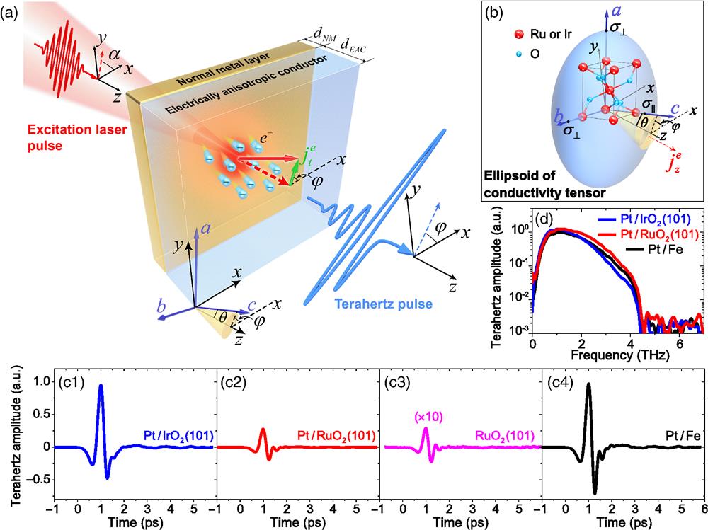
Fig. 1. Experimental setup and terahertz signals. (a) Schematic of the experimental setup. The coordinates are adapted to the laboratory frame and the lattice coordinates are labeled as . The crystal azimuthal angle , polar angle and the laser-polarization angle are defined. Femtosecond-laser-induced electrons are injected from the NM layer, resulting in transient electron currents along . In the experiment, the excitation pulse is primarily incident from the EAC layer side. However, for ease of illustration, it is depicted as incident from the NM layer side. Owing to the electrical anisotropy in the EAC layer, transverse electron currents () are generated flowing at an angle of relative to the axis. Inset: illustration of superdiffusive electron currents induced by laser-pulse excitation. (b) Schematic of the ellipsoid of conductivity tensor of and in the laboratory frame, displaying anisotropy in electrical conductivities (). The schematic uses the same coordinate and angle definitions as described in panel (a). (c) Terahertz waveforms generated from (c1) , (c2) , (c3) , and (c4) Pt/Fe devices. The signal from the thin film is scaled 10 times for comparison. (d) Terahertz spectra obtained via fast Fourier transform (FFT) of the waveforms in panel (c).
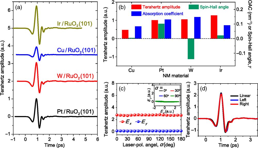
Fig. 2. Effect of NM materials and laser polarization states. (a) Terahertz waveforms generated by devices with NM materials of Ir, Cu, W, and Pt. The thickness of the NM layer is 2 nm. (b) Terahertz signal amplitude as a function of the NM materials used for the devices (red bars). For comparison, OACs at the laser wavelength of (blue bars) and spin-Hall angles (green bars) of the respective NM materials are also shown. (c) Terahertz signal amplitudes of the and components from the device as a function of the polarization angle of the linearly polarized excitation laser. Inset: projection of the terahertz waves for different values of . (d) Terahertz waveforms from the device excited by excitation pulses with linear, right- and left-circular polarizations.
Fig. 3. Effect of crystal orientations. (a) and components of terahertz waveforms generated by devices with different crystal orientations and polar angles . (b) and components of terahertz waveforms generated by at different azimuthal angles while keeping fixed at 34.7 deg. (c) Terahertz signal amplitude of and components from the device at different azimuthal angles . The solid lines represent the sine and cosine fitting to the results.
Fig. 4. Optimizing the conversion efficiency. (a) Terahertz signal amplitude as a function of incident laser fluence from the , , and Pt/Fe samples. The red and blue dashed lines represent the linear fits to the low-fluence experimental results of and , respectively. The slope of the red dashed line is times of that of the blue dashed line. (b) Terahertz signal amplitude as a function of thickness of the layer () of the device. (c) Terahertz signal amplitude as a function of thickness of the Pt layer () of the device. The solid lines in (b) and (c) represent a global fit using the thickness-dependent model (see Appendix C).
| () | () | | | | 8.13 | 8.63 | 34.7 | 0.028 | | 3.18 | 4.22 | 35.0 | 0.139 |
|
Table 1. Longitudinal (σ∥) and transverse (σ⊥) conductivities, crystal polar angles θ, and the coefficients of electrical anisotropy β0 of RuO2(101) and IrO2(101).