• Journal of Semiconductors
  • Vol. 42, Issue 8, 082901 (2021)
Zeguo Song1, Yunkun Wang1, Yunke Zhu1, Peng Bai1, An Hu1, and Yunan Gao1、2、3
Author Affiliations
  • 1State Key Laboratory for Artificial Microstructure and Mesoscopic Physics, School of Physics, Peking University, Beijing 100871, China
  • 2Frontiers Science Center for Nano-optoelectronics, Beijing 100871, China
  • 3Collaborative Innovation Center of Extreme Optics, Shanxi University, Taiyuan 030006, China
  • show less
    DOI: 10.1088/1674-4926/42/8/082901 Cite this Article
    Zeguo Song, Yunkun Wang, Yunke Zhu, Peng Bai, An Hu, Yunan Gao. Targeted transfer of self-assembled CdSe nanoplatelet film onto WS2 flakes to construct hybrid heterostructures[J]. Journal of Semiconductors, 2021, 42(8): 082901 Copy Citation Text show less
    (Color online) (a) Absorption and photoluminescence spectra of the CdSe nanoplatelets. (b) Transmission electron microscopy (TEM) image of the nanoplatelets. (c) Schematic of PDMS assisted transferring method. (d) A bright-field microscopy image of a single layer of the CdSe nanoplatelet film on a SiO2/Si substrate with WS2 flakes. (e) Photoluminescence microscopy image of CdSe films with one, two and three layers of nanoplatelets.
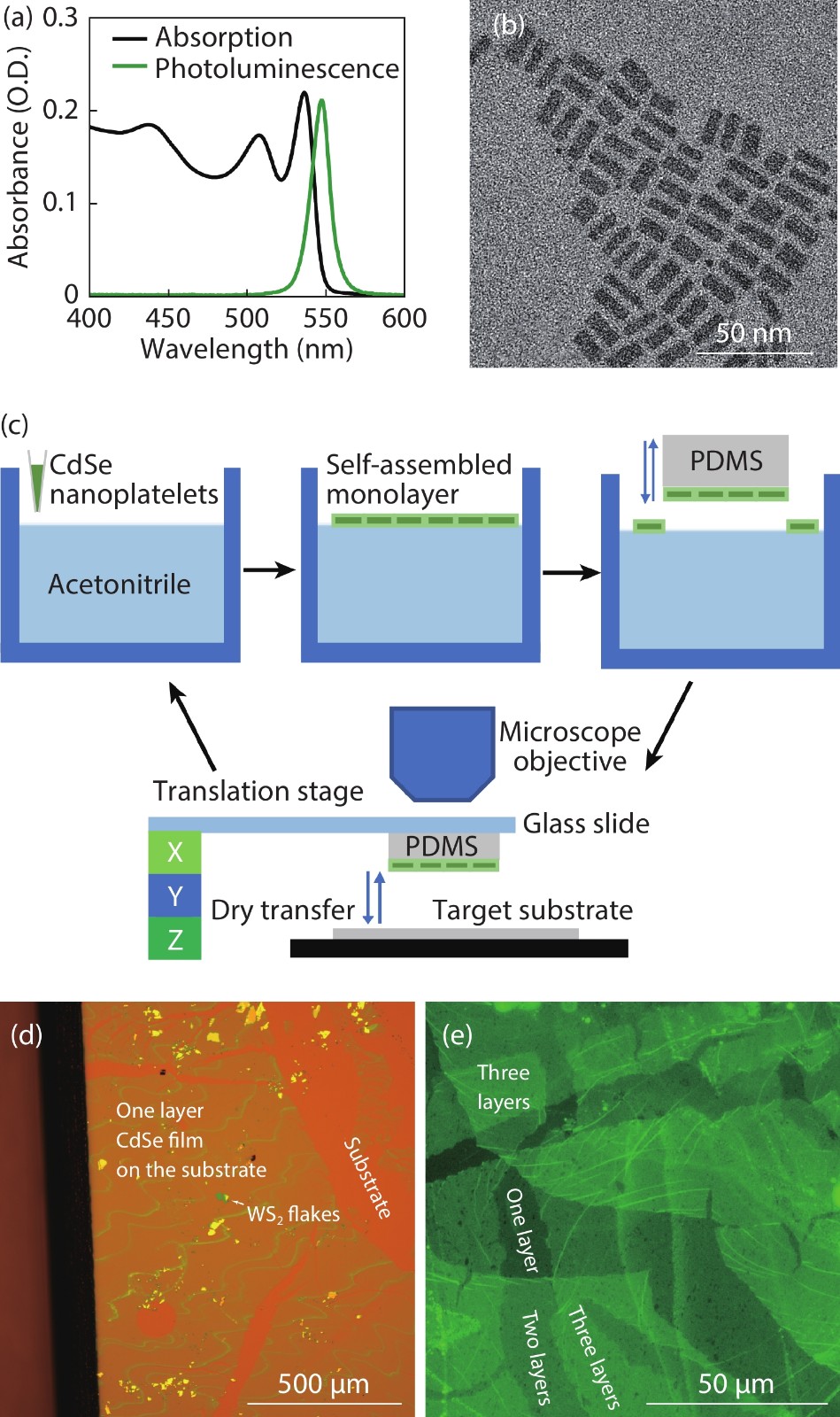
    Fig. 1. (Color online) (a) Absorption and photoluminescence spectra of the CdSe nanoplatelets. (b) Transmission electron microscopy (TEM) image of the nanoplatelets. (c) Schematic of PDMS assisted transferring method. (d) A bright-field microscopy image of a single layer of the CdSe nanoplatelet film on a SiO2/Si substrate with WS2 flakes. (e) Photoluminescence microscopy image of CdSe films with one, two and three layers of nanoplatelets.
    (Color online) (a) Photoluminescence microscopy image of a layer CdSe film transferred on a cover glass. (b, c) TEM images of a film on a SiN substrate: (b) panel (lower magnification) shows the homogeneity, and several voids are pointed out by dashed circles; (c) panel (higher magnification) shows that nanoplatelets have dominant in-plane orientation of about 90%, and the inset displayed a zoomed-in portion with nanoplatelets in edge-up (circled in dashed lines) and face-down orientations.
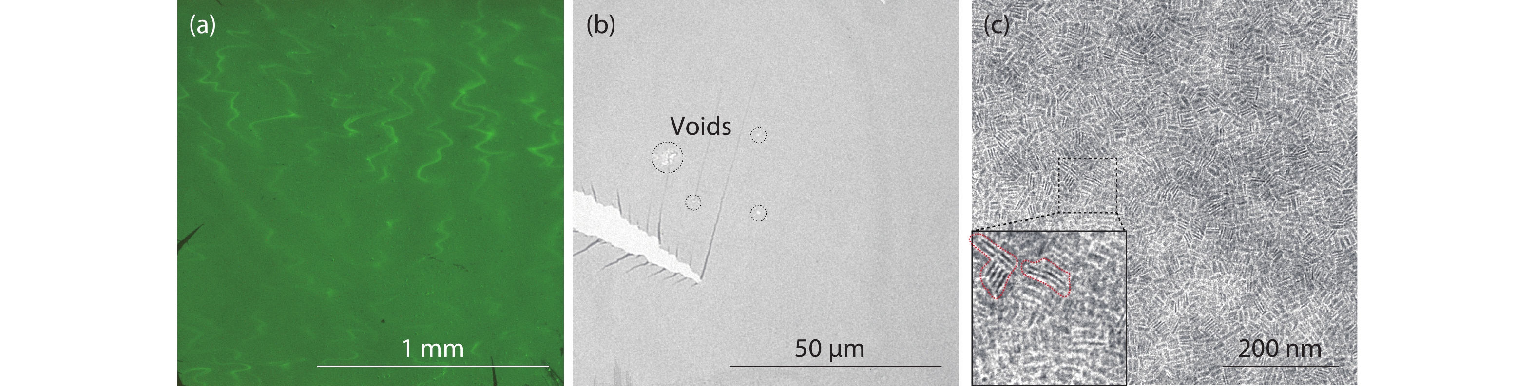
    Fig. 2. (Color online) (a) Photoluminescence microscopy image of a layer CdSe film transferred on a cover glass. (b, c) TEM images of a film on a SiN substrate: (b) panel (lower magnification) shows the homogeneity, and several voids are pointed out by dashed circles; (c) panel (higher magnification) shows that nanoplatelets have dominant in-plane orientation of about 90%, and the inset displayed a zoomed-in portion with nanoplatelets in edge-up (circled in dashed lines) and face-down orientations.
    (Color online) (a) AFM image of a CdSe nanoplatelet monolayer film transferred on a cover glass. (b) Height histography of panel a, two peaks correspond to the bare glass and the height of the film. (c) Back focal plane image of the film. (d) Comparison between simulation and experimental BFP results along the dashed crossline in panel c.
    Fig. 3. (Color online) (a) AFM image of a CdSe nanoplatelet monolayer film transferred on a cover glass. (b) Height histography of panel a, two peaks correspond to the bare glass and the height of the film. (c) Back focal plane image of the film. (d) Comparison between simulation and experimental BFP results along the dashed crossline in panel c.
    (Color online) (a) Up-left panel is an optical microscopy image of WS2 flakes on SiO2/Si, and down-right panel is an AFM image of single-layer CdSe nanoplatelets transferred on the WS2 flakes. (b) Wide field photoluminescence image of the CdSe film on/off the WS2 flakes, and the insets show the intensity change along the dashed white lines. (c) Time- and wavelength-resolved photoluminescence images measured by a streak camera. (d) Integrated intensity decay traces over the emission band in panel c, and biexponential functions are used to fit the decay traces. (e) Similar measurements as in panel c but with a shorter detection window and higher time resolution. (f) Comparison of photoluminescence decay of CdSe nanoplatelets on monolayer and trilayer WS2.
    Fig. 4. (Color online) (a) Up-left panel is an optical microscopy image of WS2 flakes on SiO2/Si, and down-right panel is an AFM image of single-layer CdSe nanoplatelets transferred on the WS2 flakes. (b) Wide field photoluminescence image of the CdSe film on/off the WS2 flakes, and the insets show the intensity change along the dashed white lines. (c) Time- and wavelength-resolved photoluminescence images measured by a streak camera. (d) Integrated intensity decay traces over the emission band in panel c, and biexponential functions are used to fit the decay traces. (e) Similar measurements as in panel c but with a shorter detection window and higher time resolution. (f) Comparison of photoluminescence decay of CdSe nanoplatelets on monolayer and trilayer WS2.
    Zeguo Song, Yunkun Wang, Yunke Zhu, Peng Bai, An Hu, Yunan Gao. Targeted transfer of self-assembled CdSe nanoplatelet film onto WS2 flakes to construct hybrid heterostructures[J]. Journal of Semiconductors, 2021, 42(8): 082901
    Download Citation