
Zeguo Song, Yunkun Wang, Yunke Zhu, Peng Bai, An Hu, Yunan Gao. Targeted transfer of self-assembled CdSe nanoplatelet film onto WS2 flakes to construct hybrid heterostructures[J]. Journal of Semiconductors, 2021, 42(8): 082901
- Journal of Semiconductors
- Vol. 42, Issue 8, 082901 (2021)
Abstract
1. Introduction
Colloidal semiconductor nanocrystals have been intensively studied for several decades, and various types in chemical compositions, shapes and sizes can be synthesized[
For controlling these nanocrystals to build macro-scale functional materials, self-assembly of them has been considered as the most promising method[
In this work, we report a fascinate method that can pick up the self-assembled single-layer CdSe films suspended on acetonitrile and then precisely transfer onto targeted substrates. Combining transmission electron microscopy (TEM), atomic force microscopy (AFM) and back focal plane imaging (BFP), we determined that the films exhibit an around 90% in-plane transition dipole distribution. Using this method, it is very convenient to construct hybrid heterostructure combining colloidal quantum dots with other structures and/or materials, in which new properties can be exploited[
2. Methods
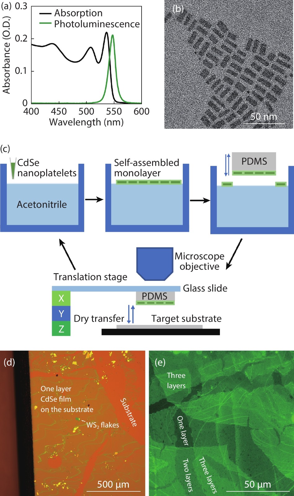
CdSe nanoplatelets were synthesized following Ref. [25], and the absorption and photoluminescence spectra are presented in Fig. 1(a). A TEM image of these nanoplatelets all laying face-down on a TEM grid is presented in Fig. 1(b), from which the length and width are determined to be 18 × 5 nm2. The thickness of the nanoplatelets is 1.5 nm, which has been well documented in literature for CdSe nanoplatelets with the emission peak at 550 nm[
![]()
Figure 1.(Color online) (a) Absorption and photoluminescence spectra of the CdSe nanoplatelets. (b) Transmission electron microscopy (TEM) image of the nanoplatelets. (c) Schematic of PDMS assisted transferring method. (d) A bright-field microscopy image of a single layer of the CdSe nanoplatelet film on a SiO2/Si substrate with WS2 flakes. (e) Photoluminescence microscopy image of CdSe films with one, two and three layers of nanoplatelets.
Atomic force microscopy (AFM) images were measured by an Oxford Cypher ES AFM. Back focal plane images were collected with the same instrument in our previous work of Ref. [18]. Time resolve photoluminescence spectra were collected by a streak camera (Hamamatsu C5680-04). The samples were excited at 415 nm under 3.8 MHz by using a 76 MHz femtosecond Ti:sapphire oscillator (fundamental 830 nm and frequency-doubled by a BBO crystal to 415 nm, and the repetition frequency lowered by a pulse picker). The laser spot is about 1 μm in diameter. Photoluminescent signals were filtered by a 450 nm long pass filter to separate the emission of the nanoplatelets from the excitation light. The photoluminescent emission images were taken by a CCD camera in a microscopy under excitation of a 395 nm LED lamp. TEM images were collected by a FEI Tecnai T20 with an accelerating voltage of 200 kV.
3. Results and discussion
Fig. 2 shows a photoluminescence microscopy image of a CdSe nanoplatelet film successfully transferred on a cover glass, which reaches an area of larger than 7 mm2. Although there are brighter stripes, it can be easily found in areas with lengths and widths of several hundreds of micrometers which show even brightness meaning a homogenous film. Fig. 2(b) shows a TEM image of a film transferred on a SiN window supported on Si. It shows an even contrast through the film together with a particularly selected crack to show the contrast. Scattered voids can be noticed. A TEM image with a higher magnification is presented in Fig. 2(c), from which the nanoplatelet orientation can be analyzed. The majority of nanoplatelets have a face-down orientation, while side-up orientation nanoplatelets can be found in scattered spots, as shown in the inset. We calculated the total area of these spots that occupies 13% of the total area. This result agrees with the recent study of Momper et al. that fast evaporation of solvent leads to that CdSe nanoplatelets have face-down orientation on acetonitrile surface[
![]()
Figure 2.(Color online) (a) Photoluminescence microscopy image of a layer CdSe film transferred on a cover glass. (b, c) TEM images of a film on a SiN substrate: (b) panel (lower magnification) shows the homogeneity, and several voids are pointed out by dashed circles; (c) panel (higher magnification) shows that nanoplatelets have dominant in-plane orientation of about 90%, and the inset displayed a zoomed-in portion with nanoplatelets in edge-up (circled in dashed lines) and face-down orientations.
To characterize the film thickness and flatness, an area with a crack was scanned using atomic force microscopy, as shown in Fig. 3(a). The image mostly has the same contrast with noticeable scattered darker voids where no nanoplatelets cover the substrate. Similar voids are also noticeable in the results of recent studies where liquid surface assembly was used[
![]()
Figure 3.(Color online) (a) AFM image of a CdSe nanoplatelet monolayer film transferred on a cover glass. (b) Height histography of panel a, two peaks correspond to the bare glass and the height of the film. (c) Back focal plane image of the film. (d) Comparison between simulation and experimental BFP results along the dashed crossline in panel c.
Several studies have revealed that these nanoplatelets have pure in-plane dipoles[
With the controlled nanoplatelet orientation and easily obtained films bigger than hundreds of micrometers, construction of hybrid heterostructures with other materials becomes much more convenient. Herein, we chose WS2 flakes as a targeted material as it is one of two-dimensional materials under intensive studies in recent years, and study energy transfer between these two types of two-dimensional materials. In Fig. 4(a), the up-left panel shows an optical microscopy image of a WS2 flakes consisting different layers, and down-right panel presents an AFM image of the constructed heterostructure, where the WS2 layer numbers are labeled. The WS2 layers were determined by the optical contrast and the thickness is measured by AFM.
![]()
Figure 4.(Color online) (a) Up-left panel is an optical microscopy image of WS2 flakes on SiO2/Si, and down-right panel is an AFM image of single-layer CdSe nanoplatelets transferred on the WS2 flakes. (b) Wide field photoluminescence image of the CdSe film on/off the WS2 flakes, and the insets show the intensity change along the dashed white lines. (c) Time- and wavelength-resolved photoluminescence images measured by a streak camera. (d) Integrated intensity decay traces over the emission band in panel c, and biexponential functions are used to fit the decay traces. (e) Similar measurements as in panel c but with a shorter detection window and higher time resolution. (f) Comparison of photoluminescence decay of CdSe nanoplatelets on monolayer and trilayer WS2.
Fig. 4(b) presents a photoluminescence microscopy image (measured at 550 nm with a band width of 17 nm) of the hybrid heterostructure and the area around with pure single-layer CdSe nanoplatelet. It clearly shows that with WS2 flakes underneath the nanoplatelet film has much lower photoluminescence intensity seen as the darker area. Two insets show the intensity change along the dashed lines. We calculated that monolayer WS2 decreases the photoluminescence intensity of the nanoplatelets to 33% while triple-layer to 22% and the much thicker layer to 7%. This photoluminescence decrease is due to energy transfer from the CdSe nanoplatelet to WS2 flakes, since the WS2 flakes have a lower energy band gap. Direct charge carrier transfer can be excluded as these CdSe nanoplatelets have capping ligands of oleic acid of about 2 nm length.
The energy transfer rate in these hybrid heterostructures have been reported with a broad variation in literature[
Fig. 4(c) presents two photoluminescence decay images of the nanoplatelet film on bare substrates and on the monolayer WS2 region. Clear shortened decay can be seen. The total intensity decay traces over the emission band are shown in Fig. 4(d). A biexponential decay function can well fit the decay traces. The fitting extracted two components of with decay time of 53 ± 3 ps and 587 ± 14 ps on the bare substrate while 50 ± 3 ps and 380 ± 8 ps on monolayer WS2. The decay time of the faster component is the same, and from the change of the decay time of the slower component the energy transfer rate can be calculated as 4.3 ns–1 by
Fig. 4(f) compares normalized decay traces of the nanoplatelets on monolayer and trilayer WS2 showing no noticeable difference in this time range. Though the trilayer WS2 quenches the steady state photoluminescence of CdSe nanoplatelets by 10% more (Fig. 4(b)), apparently it does not noticeably change the energy transfer rate in this heterostructure. It has been observed that thinner MoS2 acceptor layers lead to more efficient energy transfer from CdSe quantum dot donor, while graphene shows a contrary trend[
4. Conclusion
We developed a PDMS-assisted transferring method that can conveniently pick up self-assembled CdSe nanoplatelets from acetonitrile surface and precisely transfer to a targeted substrate. Using the method, a hybrid heterostructure of CdSe nanoplatelets and WS2 flakes was constructed, in which the nanoplatelets have 90% in-plane orientation. By using a streak camera with ps time resolution, the energy transfer rate between the nanoplatelets and the WS2 flakes is accurately determined.
Acknowledgements
This project is supported by Beijing Natural Science Foundation (grant no. Z190005), the National Natural Science Foundation of China (grant nos. 61875002) and the National Key R&D Program of China (grant no. 2018YFA0306302).
References
[1] M V Kovalenko, L Manna, A Cabot et al. Prospects of nanoscience with nanocrystals. ACS Nano, 9, 1012(2015).
[2] Y N Gao, M C Weidman, W A Tisdale. CdSe nanoplatelet films with controlled orientation of their transition dipole moment. Nano Lett, 17, 3837(2017).
[3] S Ithurria, M D Tessier, B Mahler et al. Colloidal nanoplatelets with two-dimensional electronic structure. Nat Mater, 10, 936(2011).
[4] R Scott, J Heckmann, A V Prudnikau et al. Directed emission of CdSe nanoplatelets originating from strongly anisotropic 2D electronic structure. Nat Nanotechnol, 12, 1155(2017).
[5] W D Kim, D Kim, D E Yoon et al. Pushing the efficiency envelope for semiconductor nanocrystal-based electroluminescence devices using anisotropic nanocrystals. Chem Mater, 31, 3066(2019).
[6] Z Yang, M Pelton, I Fedin et al. A room temperature continuous-wave nanolaser using colloidal quantum wells. Nat Commun, 8, 143(2017).
[7] J Q Grim, S Christodoulou, F Di Stasio et al. Continuous-wave biexciton lasing at room temperature using solution-processed quantum wells. Nat Nanotechnol, 9, 891(2014).
[8] U Giovanella, M Pasini, M Lorenzon et al. Efficient solution-processed nanoplatelet-based light-emitting diodes with high operational stability in air. Nano Lett, 18, 3441(2018).
[9] F J Zhang, S J Wang, L Wang et al. Super color purity green quantum dot light-emitting diodes fabricated by using CdSe/CdS nanoplatelets. Nanoscale, 8, 12182(2016).
[10] M A Boles, M Engel, D V Talapin. Self-assembly of colloidal nanocrystals: From intricate structures to functional materials. Chem Rev, 116, 11220(2016).
[11] X Li, Z L Lu, T Wang. Self-assembly of semiconductor nanoparticles toward emergent behaviors on fluorescence. Nano Res, 14, 1233(2021).
[12] D Vanmaekelbergh. Self-assembly of colloidal nanocrystals as route to novel classes of nanostructured materials. Nano Today, 6, 419(2011).
[13] A Dong, J Chen, P M Vora et al. Binary nanocrystal superlattice membranes self-assembled at the liquid-air interface. Nature, 466, 474(2010).
[14] B Abécassis, M D Tessier, P Davidson et al. Self-assembly of CdSe nanoplatelets into giant micrometer-scale needles emitting polarized light. Nano Lett, 14, 710(2014).
[15] O Erdem, S Foroutan, N Gheshlaghi et al. Thickness-tunable self-assembled colloidal nanoplatelet films enable ultrathin optical gain media. Nano Lett, 20, 6459(2020).
[16] R Momper, H Zhang, S Chen et al. Kinetic control over self-assembly of semiconductor nanoplatelets. Nano Lett, 20, 4102(2020).
[17] O Erdem, K Gungor, B Guzelturk et al. Orientation-controlled nonradiative energy transfer to colloidal nanoplatelets: Engineering dipole orientation factor. Nano Lett, 19, 4297(2019).
[18] P Bai, A Hu, Y Liu et al. Printing and
[19] O Özdemir, I Ramiro, S Gupta et al. High sensitivity hybrid PbS CQD-TMDC photodetectors up to 2
[20] F Prins, D K Kim, J Cui et al. Direct patterning of colloidal quantum-dot thin films for enhanced and spectrally selective out-coupling of emission. Nano Lett, 17, 1319(2017).
[21] Z He, B Chen, Y Hua et al. CMOS compatible high-performance nanolasing based on perovskite-SiN hybrid integration. Adv Opt Mater, 8, 2000453(2020).
[22] D Prasai, A R Klots, A Newaz et al. Electrical control of near-field energy transfer between quantum dots and two-dimensional semiconductors. Nano Lett, 15, 4374(2015).
[23] A Dutta, A Medda, R Bera et al. Hybrid nanostructures of 2D CdSe nanoplatelets for high-performance photodetector using charge transfer process. ACS Appl Nano Mater, 3, 4717(2020).
[24] C E Rowland, I Fedin, H Zhang et al. Picosecond energy transfer and multiexciton transfer outpaces Auger recombination in binary CdSe nanoplatelet solids. Nat Mater, 14, 484(2015).
[25] C X She, I Fedin, D S Dolzhnikov et al. Low-threshold stimulated emission using colloidal quantum wells. Nano Lett, 14, 2772(2014).
[26] T Paik, D K Ko, T R Gordon et al. Studies of liquid crystalline self-assembly of GdF3 nanoplates by in-plane, out-of-plane SAXS. ACS Nano, 5, 8322(2011).
[27] J A Schuller, S Karaveli, T Schiros et al. Orientation of luminescent excitons in layered nanomaterials. Nat Nanotechnol, 8, 271(2013).
[28] N Taghipour, P L Hernandez Martinez, A Ozden et al. Near-unity efficiency energy transfer from colloidal semiconductor quantum wells of CdSe/CdS nanoplatelets to a monolayer of MoS2. ACS Nano, 12, 8547(2018).
[29] F Prins, A J Goodman, W A Tisdale. Reduced dielectric screening and enhanced energy transfer in single- and few-layer MoS2. Nano Lett, 14, 6087(2014).
[30] A Raja, A Montoya−Castillo, J Zultak et al. Energy transfer from quantum dots to graphene and MoS2: The role of absorption and screening in two-dimensional materials. Nano Lett, 16, 2328(2016).
[31] H Liu, T Wang, C Wang et al. Exciton radiative recombination dynamics and nonradiative energy transfer in two-dimensional transition-metal dichalcogenides. J Phys Chem C, 123, 10087(2019).

Set citation alerts for the article
Please enter your email address
© Copyright 2018-2021 | Chinese Laser Press. All Rights Reserved 沪ICP备15018463号-20