
Jin-Feng Zhang, Jia-Min Xu, Ze-Yang Ren, Qi He, Sheng-Rui Xu, Chun-Fu Zhang, Jin-Cheng Zhang, Yue Hao. Characteristics of hydrogen-terminated single crystalline diamond field effect transistors with different surface orientations [J]. Acta Physica Sinica, 2020, 69(2): 028101-1
- Acta Physica Sinica
- Vol. 69, Issue 2, 028101-1 (2020)
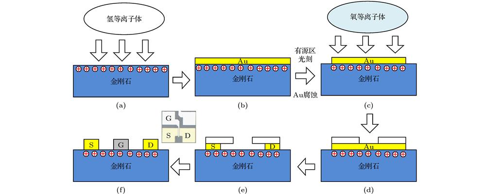
Fig. 1. Schematic diagram of the device fabrication process: (a) Hydrogen plasma treatment; (b) gold deposition; (c) device isolation; (d) gate window photolithography; (e)wet etching of gold; (f) aluminum deposition and lifting off. The inset at the upper right corner of (f) is the top view of the device.器件制备流程图 (a)氢等离子体处理; (b) Au沉积; (c)隔离工艺; (d)栅窗口光刻; (e) Au腐蚀; (f) Al沉积及剥离, 右上角为器件俯视图显微照片
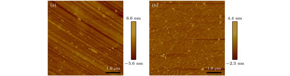
Fig. 2. Surface morphology of the diamond before hydrogen plasma treatment: (a) (110) plane; (b) (111) plane.氢等离子体处理前的金刚石表面形貌 (a) (110)面; (b) (111)面
Fig. 3. Surface morphology of the diamond after hydrogen plasma treatment: (a) (110) plane; (b) (111) plane.氢等离子体处理后的金刚石表面形貌 (a) (110)面; (b) (111)面
Fig. 4. (a) Raman spectra and (b) photoluminescence (PL) spectra of the diamond plates with different surface orientations.不同表面金刚石的 (a) Raman光谱图, (b) PL光谱
Fig. 5. Current-voltage characteristics of the gate-source diodes and fitting results at the forward bias: (a) and (b) are for device A; (c) and (d) are for device B.栅-源二极管的I -V 特性以及正向偏置下的拟合结果 (a) A器件I -V 特性; (b) 图(a)部分栅压区的拟合结果; (c) B器件I -V 特性; (d) 图(c)部分栅压区的拟合结果
Fig. 6. Output characteristics: (a) Device A; (b) device B.输出特性 (a)器件A; (b)器件B
Fig. 7. Transfer and transconductance characteristics: (a) Device A; (b) device B.转移特性 (a)器件A; (b)器件B
Fig. 8. Summary of the reported (a) I Dmax and (b) maximum transconductance of hydrogen-terminated diamond FETs dependent on the gate length[26,27,29-33]. The gate metal and gate dielectric are given for MOSFETs.
氢终端金刚石场效应管输出电流(a)和最大跨导(b)随栅长的变化(数据来自文献[26,27,29—33]), MOSFET器件给出了栅金属和栅介质
Fig. 9. Capacitance-voltage characteristics of the gate-source diode and the calculated hole density in the gated channel as a function of V GS: (a) Device A; (b) device B.
栅源二极管的C -V 特性以及计算出的沟道载流子浓度随V GS的变化 (a)器件A; (b)器件B


Set citation alerts for the article
Please enter your email address

© Copyright 2018-2021 | Chinese Laser Press. All Rights Reserved 沪ICP备15018463号-20