• Acta Physica Sinica
  • Vol. 69, Issue 2, 028101-1 (2020)
Jin-Feng Zhang1, Jia-Min Xu1, Ze-Yang Ren1、*, Qi He1, Sheng-Rui Xu1, Chun-Fu Zhang1, Jin-Cheng Zhang1、2, and Yue Hao1
Author Affiliations
  • 1State Key Discipline Laboratory of Wide Band-Gap Semiconductor Technology, School of Microelectronics, Xidian University, Xi’an 710071, China
  • 2Shaanxi Joint Key Laboratory of Graphene, Xi’an 710071, China
  • show less
    DOI: 10.7498/aps.69.20191013 Cite this Article
    Jin-Feng Zhang, Jia-Min Xu, Ze-Yang Ren, Qi He, Sheng-Rui Xu, Chun-Fu Zhang, Jin-Cheng Zhang, Yue Hao. Characteristics of hydrogen-terminated single crystalline diamond field effect transistors with different surface orientations[J]. Acta Physica Sinica, 2020, 69(2): 028101-1 Copy Citation Text show less

    Abstract

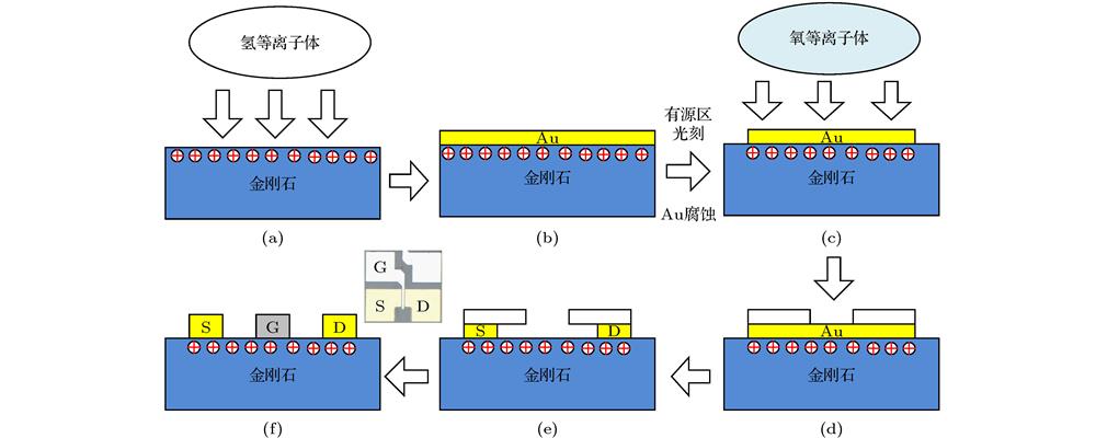
    Diamond has great potential applications in high-power, high-frequency semiconductor devices because of its wide band gap (5.5 eV), high thermal conductivity (22W/(cm·K)), and high carrier mobility (4500 cm2/(V·s) for electron, and 3800 cm2/(V·s) for hole). It has been widely considered as an ultimate semiconductor. From the analysis of our previous work, we find that the output current of field effect transistor based on hydrogen-terminated polycrystalline diamond is usually larger than that based on single crystal diamond, and that the preferential orientations of the polycrystalline diamond are mainly $ \langle 110\rangle $ and $ \langle 111\rangle $ shown by XRD results. Therefore, in order to further analyze the effect of surface orientation on the device performance of hydrogen-terminated diamond field effect transistor (FET), we study the devices fabricated respectively on the (110) plane and (111) plane single crystal diamond plates obtained from a single 3.5-mm-thick single crystal diamond grown by the microwave plasma chemical vapor deposition on the high-pressure high-temperature synthesized diamond substrate. Prior to processing the device, these diamond plates are characterized by atomic force microscope, Raman spectra and photoluminescence (PL) spectra. The results of Raman and PL spectra show that (110) plane and (111) plane plates originating from the same CVD single crystal diamond have no significant difference in optical property. Then the normally-on hydrogen-terminated diamond FET with a gate length of 6 μm is achieved. The device on (111) plane delivers a saturation drain current of 80.41 mA/mm at a gate voltage VGS = –4 V, which is approximately 1.4 times that of the device on (110) plane. Meanwhile, the on-resistance of the device on (111) plane is 48.51 Ω·mm, and it is only 67% of the device on (110) plane. Analyses of the capacitance-voltage show that the hole concentration of the gated device on (110) plane and (111) plane are 1.34 × 1013 cm–2 and 1.45 × 1013 cm–2, respectively, approximately at the same level. In addition, the hole density of the device on both (110) and (111) plane increase near-linearly with the increase of gate voltage from the threshold voltage to – 4 V, indicating that the control effect of the gate on the carrier in the channel is uniform. The possible reason for the higher saturation drain current as well as the lower on-resistance of the device on (111) plane is that its sheet resistance is lower.
    Jin-Feng Zhang, Jia-Min Xu, Ze-Yang Ren, Qi He, Sheng-Rui Xu, Chun-Fu Zhang, Jin-Cheng Zhang, Yue Hao. Characteristics of hydrogen-terminated single crystalline diamond field effect transistors with different surface orientations[J]. Acta Physica Sinica, 2020, 69(2): 028101-1
    Download Citation