• Infrared and Laser Engineering
  • Vol. 50, Issue 4, 20211023 (2021)
Baohui Zhang, Zhongwen Li, Jie Wu, Li Ji, Weiyi Wang, Lu Cai, Yahui Shi, and Jingyi Fa
Author Affiliations
  • Nanjing Research Center, Kunming Institute of Physics, Nanjing 211106, China
  • show less
    DOI: 10.3788/IRLA20211023 Cite this Article
    Baohui Zhang, Zhongwen Li, Jie Wu, Li Ji, Weiyi Wang, Lu Cai, Yahui Shi, Jingyi Fa. Design of mid-wave 1 280×1 024 infrared imaging components (Invited)[J]. Infrared and Laser Engineering, 2021, 50(4): 20211023 Copy Citation Text show less
    15 μm 1280×1024 cooled infrared imaging components. (a) Schematic diagram; (b) Exploded view
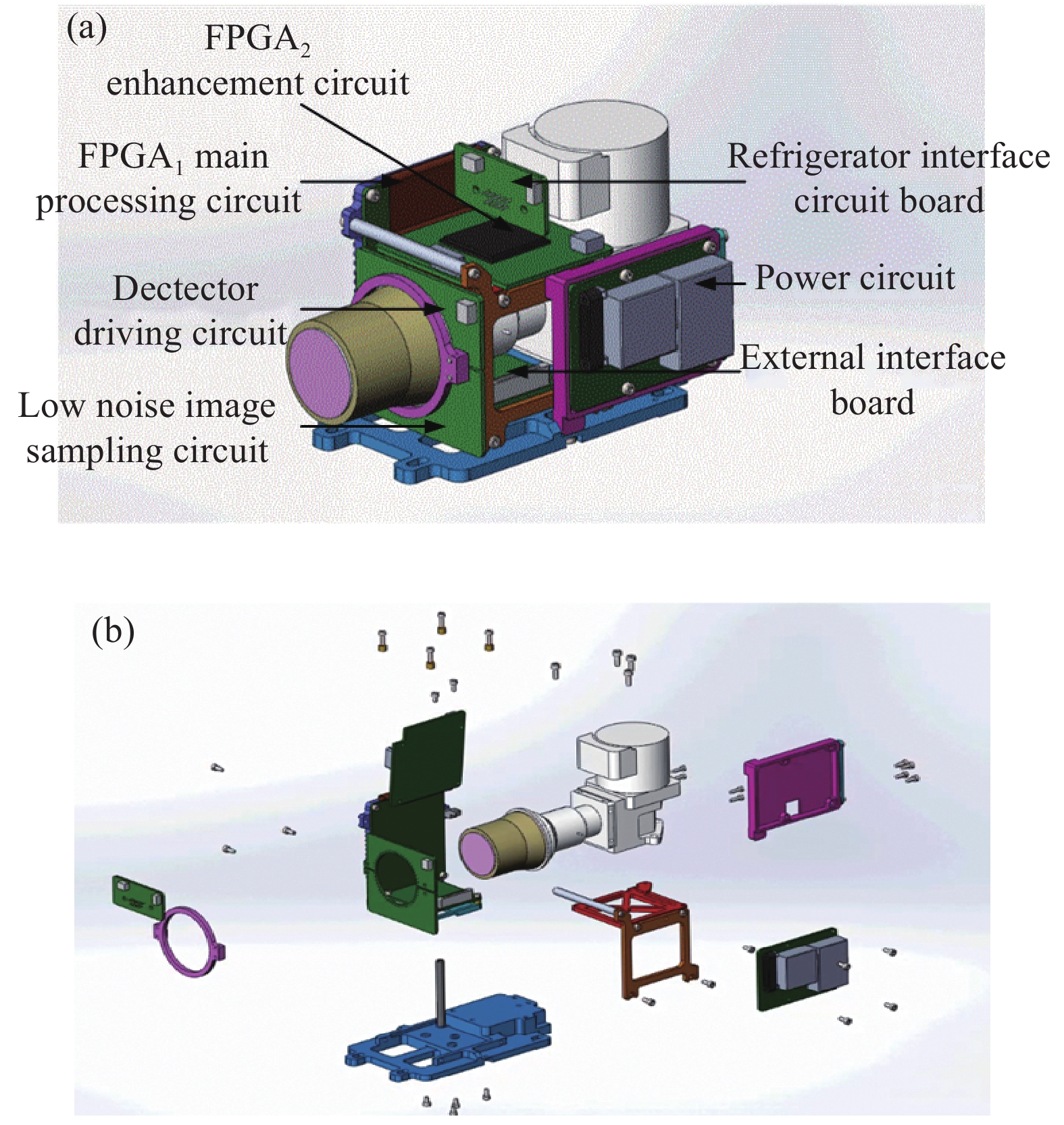
    Fig. 1. 15 μm 1280×1024 cooled infrared imaging components. (a) Schematic diagram; (b) Exploded view
    Image processing circuit hardware design
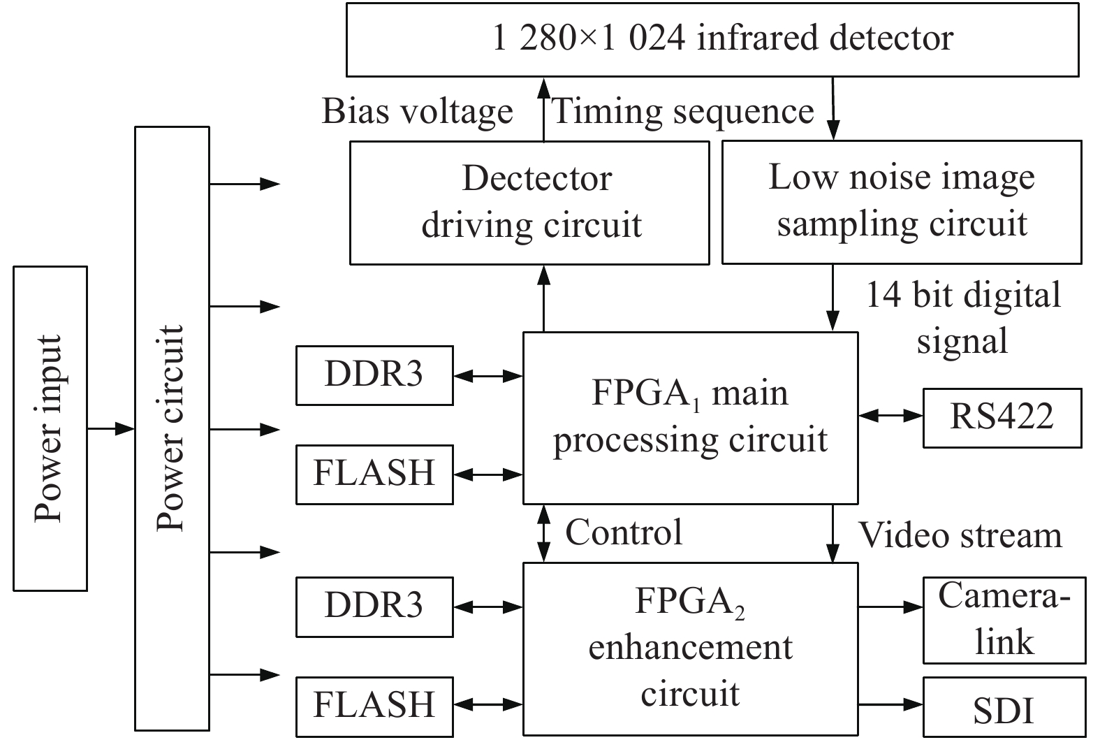
    Fig. 2. Image processing circuit hardware design
    Detector bias voltage circuit
    Fig. 3. Detector bias voltage circuit
    Low noise circuit design scheme
    Fig. 4. Low noise circuit design scheme
    Power circuit diagram
    Fig. 5. Power circuit diagram
    Design diagram of FPGA1 processing circuit program module
    Fig. 6. Design diagram of FPGA1 processing circuit program module
    Design diagram of FPGA2 enhancement board program module
    Fig. 7. Design diagram of FPGA2 enhancement board program module
    Multi-point correction temperature point selection diagram
    Fig. 8. Multi-point correction temperature point selection diagram
    Multi-point calibration temperature selection. (a) Average segmentation; (b) Adaptive segmentation
    Fig. 9. Multi-point calibration temperature selection. (a) Average segmentation; (b) Adaptive segmentation
    15 μm 1280 × 1024 cooled infrared imaging components
    Fig. 10. 15 μm 1280 × 1024 cooled infrared imaging components
    RMS value of the noise floor of the measurement circuit
    Fig. 11. RMS value of the noise floor of the measurement circuit
    Noise spectrum curve of output voltage V4
    Fig. 12. Noise spectrum curve of output voltage V4
    NETD test picture
    Fig. 13. NETD test picture
    High and low temperature imaging images. (a) −40 ℃; (b) 60 ℃
    Fig. 14. High and low temperature imaging images. (a) −40 ℃; (b) 60 ℃
    Block inhibition implementation effect diagram. (a) Before processing; (b) After processing
    Fig. 15. Block inhibition implementation effect diagram. (a) Before processing; (b) After processing
    CLAHE implementation effect diagram. (a) Traditional CLAHE; (b) Optimized CLAHE
    Fig. 16. CLAHE implementation effect diagram. (a) Traditional CLAHE; (b) Optimized CLAHE
    Digital detector imaging picture. (a) Traditional; (b) Optimized
    Fig. 17. Digital detector imaging picture. (a) Traditional; (b) Optimized
    ParameterSpecification
    Image resolution1280×1024
    Pixel picth/μm215×15
    Spectral response/μm3.7-4.8
    Work modeITR/IWR
    Signal output4 or 8
    Work temperature/℃−40-60
    Frame rate/Hz≤50
    Average NETD/mK≤ 25
    Table 1. [in Chinese]
    AlgorithmDDR3 bandwidth occupied/Gbps
    NUC inter-frame cache7.5
    Noise reduction inter-frame cache2.1
    CLAHE inter-frame cache1.6
    SDI display inter-frame cache3.4
    Table 2. [in Chinese]
    Algorithm MSE TraditionalCLAHEOptimized CLAHE
    Interested area (MSE1)5.46110.9137.36
    Total image (MSE2)2709.552716.882782.73
    Table 3. [in Chinese]
    Baohui Zhang, Zhongwen Li, Jie Wu, Li Ji, Weiyi Wang, Lu Cai, Yahui Shi, Jingyi Fa. Design of mid-wave 1 280×1 024 infrared imaging components (Invited)[J]. Infrared and Laser Engineering, 2021, 50(4): 20211023
    Download Citation