• Advanced Photonics Nexus
  • Vol. 2, Issue 2, 024002 (2023)
Matteo Cherchi, Arijit Bera, Antti Kemppinen, Jaani Nissilä, Kirsi Tappura, Marco Caputo, Lauri Lehtimäki, Janne Lehtinen, Joonas Govenius, Tomi Hassinen, Mika Prunnila, and Timo Aalto*
Author Affiliations
  • VTT Technical Research Centre of Finland Ltd., Espoo, Finland
  • show less
    DOI: 10.1117/1.APN.2.2.024002 Cite this Article Set citation alerts
    Matteo Cherchi, Arijit Bera, Antti Kemppinen, Jaani Nissilä, Kirsi Tappura, Marco Caputo, Lauri Lehtimäki, Janne Lehtinen, Joonas Govenius, Tomi Hassinen, Mika Prunnila, Timo Aalto. Supporting quantum technologies with an ultralow-loss silicon photonics platform[J]. Advanced Photonics Nexus, 2023, 2(2): 024002 Copy Citation Text show less
    Sketch of the main building blocks available on the thick-SOI platform. Typical thickness of the device layer is 3 μm, whereas the BOX thickness can vary from 400 nm to 3 μm. We define “active” building blocks as those requiring electrical pads for either control or readout.
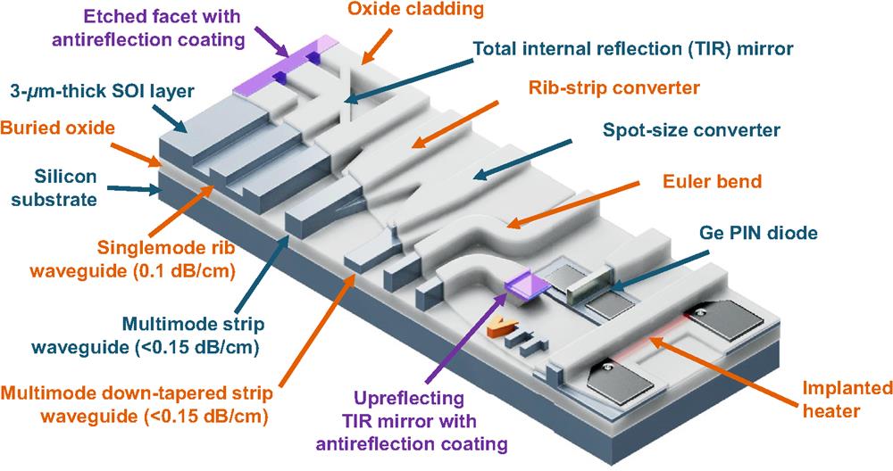
    Fig. 1. Sketch of the main building blocks available on the thick-SOI platform. Typical thickness of the device layer is 3  μm, whereas the BOX thickness can vary from 400 nm to 3  μm. We define “active” building blocks as those requiring electrical pads for either control or readout.
    (a) Sketch of different mode size conversions starting from an SMF coupled to the 3-μm thick waveguides of a thick-SOI PIC using an optical interposer fabricated on 12-μm thick SOI. The sketch also shows how the mode size can be reduced further even to couple light to submicron waveguides on a flip-chip bonded PIC that can be evanescently coupled through suitable inverse tapers. (b) Micrograph of a 12-μm thick rib waveguide of a fabricated optical interposer; (c) micrograph of a strip waveguide polished down to about 3-μm thickness on the opposite facet; (d) near-field image (infrared camera) of the TE and TM modes at the output facet of the interposer [shown in (c)]; and (e) packaged 3-μm thick-SOI PIC coupled to a fiber array through an optical interposer.
    Fig. 2. (a) Sketch of different mode size conversions starting from an SMF coupled to the 3-μm thick waveguides of a thick-SOI PIC using an optical interposer fabricated on 12-μm thick SOI. The sketch also shows how the mode size can be reduced further even to couple light to submicron waveguides on a flip-chip bonded PIC that can be evanescently coupled through suitable inverse tapers. (b) Micrograph of a 12-μm thick rib waveguide of a fabricated optical interposer; (c) micrograph of a strip waveguide polished down to about 3-μm thickness on the opposite facet; (d) near-field image (infrared camera) of the TE and TM modes at the output facet of the interposer [shown in (c)]; and (e) packaged 3-μm thick-SOI PIC coupled to a fiber array through an optical interposer.
    (a) SEM image of polymer lenses 3D printed in front of the end facets of four rib waveguides; (b) near-field picture of the output mode of a rib waveguide taken with an infrared camera; (c) near-field picture of the output of a lensed rib waveguide [same scale as (b)].
    Fig. 3. (a) SEM image of polymer lenses 3D printed in front of the end facets of four rib waveguides; (b) near-field picture of the output mode of a rib waveguide taken with an infrared camera; (c) near-field picture of the output of a lensed rib waveguide [same scale as (b)].
    (a) Micrograph of a fabricated URM and (b) side view of a vertical cross section of an URM via focused ion beam microscopy.
    Fig. 4. (a) Micrograph of a fabricated URM and (b) side view of a vertical cross section of an URM via focused ion beam microscopy.
    (a) SEM picture of 90-deg turning mirrors on rib waveguides and strip waveguides; (b) detail of a compact imbalanced MZI based on TIR mirrors; (c) SEM picture of Euler bends with L and U shape and detail of a spiral waveguide using larger L-bends.
    Fig. 5. (a) SEM picture of 90-deg turning mirrors on rib waveguides and strip waveguides; (b) detail of a compact imbalanced MZI based on TIR mirrors; (c) SEM picture of Euler bends with L and U shape and detail of a spiral waveguide using larger L-bends.
    (a) The linear change of the curvature 1/R as a function of the length s in an Euler bend, starting from zero, reaching up to 1/Rmin and then going back to zero symmetrically. (b) Example layout of a 90-deg Euler bend (or L-bend) with unity minimum bending radius, showing the resulting effective radius Reff. (c) Simulation of the transmission of the TE00 mode and of five horizontal higher-order TE modes of a 1.5-μm-wide strip waveguide at the output of a 90-deg Euler bend as a function of the minimum bending radius. The five HOM TEn0 modes (n=1,…,5) have n nodes in the horizontal direction and zero nodes in the vertical direction. The wavelength is 1.55 μm.
    Fig. 6. (a) The linear change of the curvature 1/R as a function of the length s in an Euler bend, starting from zero, reaching up to 1/Rmin and then going back to zero symmetrically. (b) Example layout of a 90-deg Euler bend (or L-bend) with unity minimum bending radius, showing the resulting effective radius Reff. (c) Simulation of the transmission of the TE00 mode and of five horizontal higher-order TE modes of a 1.5-μm-wide strip waveguide at the output of a 90-deg Euler bend as a function of the minimum bending radius. The five HOM TEn0 modes (n=1,,5) have n nodes in the horizontal direction and zero nodes in the vertical direction. The wavelength is 1.55  μm.
    (a) Sketch of an MZI exploiting the form birefringence of waveguides of different widths to serve as a PBS. (b) Scheme of a possible implementation of an integrated light circulator by combining PBSs, FRs, and reciprocal polarization rotators on chip.
    Fig. 7. (a) Sketch of an MZI exploiting the form birefringence of waveguides of different widths to serve as a PBS. (b) Scheme of a possible implementation of an integrated light circulator by combining PBSs, FRs, and reciprocal polarization rotators on chip.
    (a) Compact AWG with 100-GHz channel spacing and 5-nm free spectral range exploiting Euler bends and nearly zero birefringence waveguides, ensuring polarization-independent operation. (b) Cyclic echelle grating with 100-GHz channel spacing.
    Fig. 8. (a) Compact AWG with 100-GHz channel spacing and 5-nm free spectral range exploiting Euler bends and nearly zero birefringence waveguides, ensuring polarization-independent operation. (b) Cyclic echelle grating with 100-GHz channel spacing.
    (a) 3D simulation using the eigenmode expansion method of the adiabatic power transfer from a 3-μm thick c-Si waveguide to a 400-nm thick and 200-μm long a-Si:H tapered waveguide fabricated on top. (b) 3D sketch of two escalators to couple light to the a-Si:H waveguide and then back to the 3-μm thick waveguide, showing where a functional layer can be sandwiched between the two silicon types in the region where the light is guided in a-Si:H. (c) A different type of escalator to couple light to submicron waveguides.
    Fig. 9. (a) 3D simulation using the eigenmode expansion method of the adiabatic power transfer from a 3-μm thick c-Si waveguide to a 400-nm thick and 200-μm long a-Si:H tapered waveguide fabricated on top. (b) 3D sketch of two escalators to couple light to the a-Si:H waveguide and then back to the 3-μm thick waveguide, showing where a functional layer can be sandwiched between the two silicon types in the region where the light is guided in a-Si:H. (c) A different type of escalator to couple light to submicron waveguides.
    Top views and cross sections of the three main types of phase shifters available on the platform: (a) thermo-optic (also see Fig. 1); (b) electro-optic, based on plasma dispersion through carrier injection in a PIN junction; (c) electro-optic, based on EFIPE with a high-inverse bias voltage through a PIN junction.
    Fig. 10. Top views and cross sections of the three main types of phase shifters available on the platform: (a) thermo-optic (also see Fig. 1); (b) electro-optic, based on plasma dispersion through carrier injection in a PIN junction; (c) electro-optic, based on EFIPE with a high-inverse bias voltage through a PIN junction.
    (a) SEM picture of a fabricated NbN SNSPD before a-Si:H deposition; (b) micrograph of a detail of a fabricated chip after etching the a-Si:H waveguides; (c) sketched cross section of an a-Si:H waveguide with the NbN nanowire embedded (in green).
    Fig. 11. (a) SEM picture of a fabricated NbN SNSPD before a-Si:H deposition; (b) micrograph of a detail of a fabricated chip after etching the a-Si:H waveguides; (c) sketched cross section of an a-Si:H waveguide with the NbN nanowire embedded (in green).
    (a) Schematic representation of QKD implementations based on a central node for photon detection where all the users are equipped with suitable and low-cost transmitters. (b) 3D sketch of the solution we are developing with our partner Single Quantum to address arrays of SNSPDs with low-loss and high-fabrication yield.
    Fig. 12. (a) Schematic representation of QKD implementations based on a central node for photon detection where all the users are equipped with suitable and low-cost transmitters. (b) 3D sketch of the solution we are developing with our partner Single Quantum to address arrays of SNSPDs with low-loss and high-fabrication yield.
    Schematic representation of our plans to use optical fiber links to interface cryogenic quantum computers with supercomputers.
    Fig. 13. Schematic representation of our plans to use optical fiber links to interface cryogenic quantum computers with supercomputers.
    Long-term vision of a PIC based serializer, including an IMLL as a multiwavelength light source.
    Fig. 14. Long-term vision of a PIC based serializer, including an IMLL as a multiwavelength light source.
    Matteo Cherchi, Arijit Bera, Antti Kemppinen, Jaani Nissilä, Kirsi Tappura, Marco Caputo, Lauri Lehtimäki, Janne Lehtinen, Joonas Govenius, Tomi Hassinen, Mika Prunnila, Timo Aalto. Supporting quantum technologies with an ultralow-loss silicon photonics platform[J]. Advanced Photonics Nexus, 2023, 2(2): 024002
    Download Citation