
Matteo Cherchi, Arijit Bera, Antti Kemppinen, Jaani Nissilä, Kirsi Tappura, Marco Caputo, Lauri Lehtimäki, Janne Lehtinen, Joonas Govenius, Tomi Hassinen, Mika Prunnila, Timo Aalto, "Supporting quantum technologies with an ultralow-loss silicon photonics platform," Adv. Photon. Nexus 2, 024002 (2023)
- Advanced Photonics Nexus
- Vol. 2, Issue 2, 024002 (2023)
Abstract
Keywords
1 Introduction
We are presently living in the so-called second quantum revolution, where the focus has shifted from pure science to technologies and applications.1 Photonic technologies are expected to play a major role, not only in quantum applications but also in classical configurations to support solid-state quantum systems. In particular, photonic integrated circuits (PICs) offer unique opportunities for different quantum technologies to scale up system complexity and integration density while providing unmatched performance and stability.2
A relevant example application is large-scale deployment of quantum key distribution (QKD), for which we are developing efficient multiplexed receivers. A second interesting case is the use of our photonic integration technology to scale up superconducting quantum computers by controlling and reading out the qubits in the cryostat through classical optical links. In this case, the major challenge is the development of suitable electrical-to-optical and optical-to-electrical converters (OECs) operating at cryogenic temperatures.
We will cover these ongoing developments as follows, showing our recent results as well as our plans to further exploit the platform. In Sec. 2, we will first give an overview of the thick-silicon photonics platform, with a special focus on the most relevant features for quantum technologies. In Secs. 3 and 4, we will cover the ongoing developments for QKD and quantum computers and then conclude in Sec. 5 and briefly mention other promising future developments and applications.
Sign up for Advanced Photonics Nexus TOC. Get the latest issue of Advanced Photonics Nexus delivered right to you!Sign up now
2 Overview of VTT Thick Silicon-on-Insulator Platform
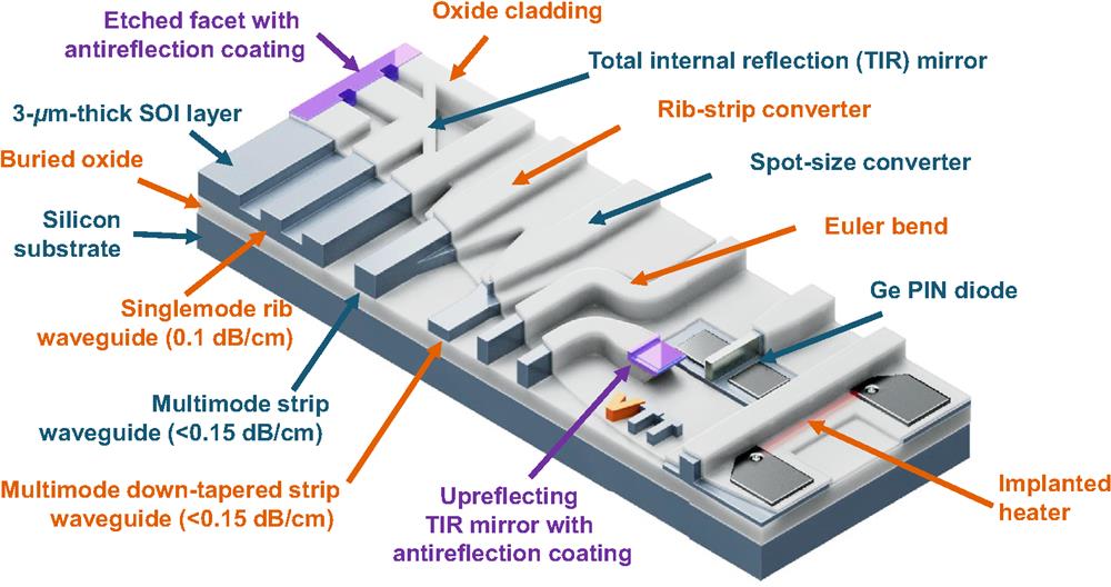
We can divide the building blocks of the platform into two main categories: passives and actives. In this context, “active” means anything requiring an electrical control, such as thermo-optic phase shifters and electro-optic modulators, or electrical readout, such as a photodiode. An overview of the main building blocks available on the platform is sketched in Fig. 1 with the notable exception of phase modulators based on PIN diodes, which are explained in detail in Sec. 2.2. We fabricate our PICs on 150-mm diameter silicon-on-insulator (SOI) wafers (to be upgraded soon to 200 mm) with
![]()
Figure 1.Sketch of the main building blocks available on the thick-SOI platform. Typical thickness of the device layer is
2.1 Passive Building Blocks
2.1.1 Types of waveguides
The five main waveguide types available on the platform are: rib waveguides, strip waveguides, down-tapered strip waveguides, strip waveguides with a thin pedestal, and down-tapered strip waveguides with a thin pedestal (the latter is the only type missing in Fig. 1). For rib waveguides, trenches are partially etched (typically
2.1.2 I/O coupling
We fabricate the vertical waveguide facets of our PICs at wafer scale by first etching the silicon facet and then depositing a suitable antireflection coating, which can be made of either a single dielectric layer or multiple layers.
The coupling loss to optical fibers can be as low as 0.5 dB, provided that the mode field diameter is about
![]()
Figure 2.(a) Sketch of different mode size conversions starting from an SMF coupled to the
![]()
Figure 3.(a) SEM image of polymer lenses 3D printed in front of the end facets of four rib waveguides; (b) near-field picture of the output mode of a rib waveguide taken with an infrared camera; (c) near-field picture of the output of a lensed rib waveguide [same scale as (b)].
Light can also be coupled to the PIC vertically from URMs (see Figs. 1 and 4), which are wet etched with a negative angle. Their working principle is total internal reflection, and coupling losses are practically the same as for the vertical facets. The antireflection coating for URMs is the same as for vertical facets. The wet etching process occurs along crystalline planes, meaning that the mirrors can be fabricated only along the four orthogonal crystal planes with Miller indices of
![]()
Figure 4.(a) Micrograph of a fabricated URM and (b) side view of a vertical cross section of an URM via focused ion beam microscopy.
Compared to grating couplers typically used in submicron waveguides, URMs support both TE and TM polarizations with negligible polarization-dependent loss, and they operate over the whole transparency range of silicon, from 1.2 to
2.1.3 Tight bends enabling high-integration density
It is generally assumed that waveguides with micron-scale cross sections require bending radii on the order of several millimeters. This is because the index contrast ensuring single-mode operation in a micron-scale waveguide would inherently lead to high radiation losses for tighter bends. In the platform, we have developed two solutions to this limitation: turning mirrors based on TIR28 [Figs. 5(a) and 5(b)] and tight adiabatic bends referred to as the Euler bends [Fig. 5(a)].11 The first approach applies to both rib waveguides and strip waveguides, whereas the second requires high-index contrast strip waveguides.
![]()
Figure 5.(a) SEM picture of 90-deg turning mirrors on rib waveguides and strip waveguides; (b) detail of a compact imbalanced MZI based on TIR mirrors; (c) SEM picture of Euler bends with L and U shape and detail of a spiral waveguide using larger L-bends.
TIR mirrors allow for compact layouts, such as the imbalanced Mach–Zehnder interferometer (MZI) shown in Fig. 5(b), which also shows the very low-loss (
For this reason, we have also developed more conventional waveguide bends to achieve much lower losses. They are based on strip waveguides, ensuring negligible radiation loss due to strong light confinement. The only limitation is that they support several HOMs that get easily excited in a tight bend. We have, therefore, introduced11 and patented30 a geometry with gradual a change of curvature, using the Euler spiral geometry as shown in Figs. 5(c), 6(a), and 6(b). This way, tight bends with loss lower than 0.02 dB can be achieved with effective bending radii of a few tens of microns, enabling, e.g., compact race track resonators with quality factor
![]()
Figure 6.(a) The linear change of the curvature
Even though, in general, the wavelength range of operation of the bends is not as wide as that of turning mirrors, bends can be designed to cover bandwidths of several hundreds of nanometers up to a few microns. An interesting property of Euler bends is that they very efficiently transmit most of supported HOMs31 (i.e., those with effective index sufficiently higher than the cladding refractive index), as highlighted in Fig. 6(c). In other words, the bends preserve the mode power distribution, which is useful when designing PICs for mode multiplexing32 and when using spatial modes as a quantum degree of freedom33
2.1.4 Polarization management
Micron-scale silicon waveguides support both TE and TM polarizations with very similar spatial mode distributions, the same propagation losses, and very similar effective indices. Indeed, strip waveguides with a square cross section can support TE and TM fundamental modes with identical propagation constants. Any possible residual birefringence induced by material strain can be easily compensated by fine-tuning the waveguide width.
Most of the building blocks, including multimode interference (MMI) splitters, can be designed to support both polarizations at the same time. On the other hand, in many applications (including telecom and sensing), polarization can be used as a degree of freedom, in which case a polarization splitter/combiner is needed and preferably also different types of polarization rotators. We are presently developing a wide portfolio of building blocks for polarization management, including MZI polarization beam splitters (PBSs)13,38 [see Fig. 7(a)] and rotators.39 Remarkably, we have demonstrated the use of silicon itself as a magneto-optic material and achieved Faraday rotation in zero-birefringence waveguides.14 Our ultimate goal is to build a fully integrated all-silicon circulator based on splitters/combiners and reciprocal and nonreciprocal rotators [Fig. 7(b)].
![]()
Figure 7.(a) Sketch of an MZI exploiting the form birefringence of waveguides of different widths to serve as a PBS. (b) Scheme of a possible implementation of an integrated light circulator by combining PBSs, FRs, and reciprocal polarization rotators on chip.
We conclude this section by mentioning that Faraday mirrors are commonly used in quantum photonics, including QKD systems (see Sec. 3), to ensure stable operation,40,41 as the polarization of the reflected light is always orthogonal to the input polarization (i.e., antipodal on the Poincaré sphere).42 Faraday mirrors can be achieved in the platform by combining an FR with a back-reflector, such as an MMI reflector or a Sagnac loop.43
2.1.5 Low-loss wavelength filters
We have demonstrated several different types of wavelength filters, including ring resonators with
![]()
Figure 8.(a) Compact AWG with 100-GHz channel spacing and 5-nm free spectral range exploiting Euler bends and nearly zero birefringence waveguides, ensuring polarization-independent operation. (b) Cyclic echelle grating with 100-GHz channel spacing.
2.1.6 Interfacing micro- and nanoscale devices
The low propagation loss of micron-scale waveguide technology comes with the price of weak interaction with any element integrated directly on top of the waveguides. This problem has been successfully addressed with different fabrication techniques that do not jeopardize the performance of the platform. For example, recently we have been developing a light escalator47 made of hydrogenated amorphous silicon (a-Si:H) to interface micron-scale waveguides with submicron waveguides, thin layers including 2D materials, and superconducting nanowires. We grow a submicron layer of a-Si:H (refractive index around 3.65) on top of the crystalline device layer (refractive index around 3.48 at a 1550 nm wavelength), and pattern it to achieve adiabatic light coupling. The simulation in Fig. 9(a) shows how the light propagates from the thick silicon waveguide to the thinner a-Si:H layer. The a-Si:H layer thickness can be optimized to maximize the overlap of the propagating light with, e.g., a graphene layer (for applications such as light detection48 or modulation49) or a superconducting nanowire single-photon detector50 (SNSPD, also see Sec. 2.2) sandwiched between crystalline silicon (c-Si) and a-Si:H, similar to what is sketched in Fig. 9(b). Furthermore, crystalline silicon can also be selectively removed and replaced with a deposited silica layer before depositing the a-Si:H layer, as sketched in Fig. 9(c). The resulting high-index contrast a-Si:H waveguide allows us to interface the micron-scale waveguide with submicron waveguides including plasmonic slot waveguides or even just PICs based on submicron silicon waveguides that can be simply bonded on top of the a-Si:H waveguide and evanescently coupled via inverse tapers. Both types of escalators can be fabricated using the same fabrication process. Another unique opportunity to couple microscale waveguides to nanophotonic devices comes from the URM. In fact, there are cases requiring the light to propagate across a functional surface (unlike the escalator case, where it propagates along it). In these cases, functional surfaces can be fabricated or just transferred on top of the flat output surface of the mirror (which is made of crystalline smooth silicon, not etched). This is a straightforward way to integrate metasurfaces, including waveplates,51 metalenses,52 or electro-optic modulators.53,54 However, the limited size of the mirror (
![]()
Figure 9.(a) 3D simulation using the eigenmode expansion method of the adiabatic power transfer from a
2.2 Active Building Blocks
We can divide the active elements in two main categories: electrical-to-optical converters (EOCs), which, in the thick-SOI platform, are basically all phase shifters (either thermo-optic or electro-optic) and OECs, i.e., photodetectors.
2.2.1 Phase shifters
We implement thermo-optic phase shifters by implanting a thin silicon pedestal at the bottom of strip waveguides [Fig. 10(a)]. We usually cut away the remaining part of the pedestal to achieve lower power consumption, reaching about 25 mW per
![]()
Figure 10.Top views and cross sections of the three main types of phase shifters available on the platform: (a) thermo-optic (also see
Placing the heaters in direct contact with the silicon layer ensures a significant reduction of thermal cross talk55 compared to heaters based on metal wires placed on top of the waveguide upper cladding. This is a major advantage for complex circuits requiring several thermo-optic phase shifters. By design, thermo-optic phase shifters come with no excess loss.
When higher speed is needed, we can reach about 2–3 MHz using simple PIN junctions, with only one implantation level, as sketched in Fig. 10(b). In this case, the refractive index changes due to carrier injection inducing plasma dispersion.56 The power consumption for a
To overcome these limitations, we are also developing phase modulators relying on the so-called electric-field-induced Pockels effect [EFIPE, see Fig. 10(c)],58 in close collaboration with the University of Tokyo. For these modulators, we expect significantly lower excess loss due to the high-reverse bias (electric field of about
With the goal of achieving extremely low-power consumption in combination with modulation speeds exceeding 100 GHz, we are also developing plasmonic modulators in collaboration with ETH Zürich and the company Polariton Technologies.61 In addition to the conventional approach based on nonlinear polymers, we are also exploring the possible use of a-Si:H as nonlinear material based on EFIPE.62 We point out that plasmonic modulators are also particularly suitable for cryogenic applications,63 since they do not rely on charge carriers and operate with ultralow power dissipation.64 The main limitation of plasmonic phase shifters is the high excess loss, typically exceeding 5 dB. However, as explained in Sec. 3, this can be acceptable in some applications.
To conclude this section, we point out that a key missing building block for quantum PICs (QPICs) in all platforms is a suitable phase shifter to simultaneously enable a small footprint, ultralow power consumption, high-speed, ultralow optical loss, and cryogenic operation, or at least a subset of these properties, depending on the application. Recent results demonstrate that using microelectromechanical systems is a promising path for both submicron silicon65 and silicon nitride66,67 platforms. This approach can result in losses below 0.5 dB, speeds from a few MHz to beyond 100 MHz, and footprints ranging from about
2.2.2 Detectors
The platform includes monolithically integrated germanium (Ge) photodiodes (PD), with responsivity on the order of
Additionally, in collaboration with ETH Zürich, we are also developing high-speed plasmonic Ge detectors to exceed 500 GHz analog bandwidth.74,75 Here the main driver is not the detection efficiency but high-speed operation at a few deg. Kelvin, with the goal of developing suitable OECs to transfer a large amount of data to the cryostat. As explained in more detail in Sec. 4, the idea is to drive superconducting electronics (e.g., single-flux quantum, SFQ) using optical fibers.
With cryogenic and quantum applications in mind, we are also developing guided-wave SNSPDs, with the final goal of coupling them through a light escalator [Fig. 9(b)]. In order to speed up the detector development, we have started fabricating the devices sketched in Fig. 11(c). We first oxidized a silicon wafer, deposited superconducting NbN on the thermal oxide, and patterned the nanowires using e-beam lithography, as shown in Fig. 11(a). Next, we deposited a-Si:H and patterned the waveguides [Fig. 11(b)] including inverse tapers to improve fiber coupling from the chip edge. The optical fiber is aligned using a nanopositioner in the cryostat. In parallel, we are also developing amorphous alternatives76,77 to crystalline NbN, targeting improved fabrication yield of the detectors.
![]()
Figure 11.(a) SEM picture of a fabricated NbN SNSPD before a-Si:H deposition; (b) micrograph of a detail of a fabricated chip after etching the a-Si:H waveguides; (c) sketched cross section of an a-Si:H waveguide with the NbN nanowire embedded (in green).
The SNSPD is the closest thing to an ideal single-photon detector demonstrated to date, with detection efficiencies exceeding 97% extending into the telecom wavelength range,78 speeds in the GHz range,79 jitter even lower than 3 ps,80 and dark counts under 0.1 Hz.81 However, for some quantum realizations,82
However, it should be noted here that solid-state cooling technology developed currently at VTT can provide a viable solution to integrate also compact sub-Kelvin refrigerators in the future.86,87 These coolers are superconductor—silicon hybrid chips that can be directly connected to the PIC with 3D-integration schemes, such as flip-chip bonding. This would enable sub-Kelvin operation temperature for the circuits inside simple, cost-effective, and compact pulse-tube systems.
Integration of TESs on optical waveguides has already been demonstrated on other platforms.88,89 Our integration approach is in line with what we explained above for SNSPDs and leverages the TES pixel90 and SQUID-based readout technology91 developed at VTT. From a broader perspective, the in-house integrated superconducting device technology based on Nb cross junctions92 can provide interesting opportunities for the quantum upgrade of the micron-scale platform (also see Sec. 4). For example, we presently use the technology for the TES readout circuits,89 SQUID magnetometers,93 and different Josephson parametric devices.94
2.3 Hybrid Integration
Several different PIC technologies are available, including most mature submicron and micron-scale silicon and silicon nitride20 platforms, and micron-scale indium phosphide100 platforms, as well as the more recent lithium niobate on-insulator platforms101
Our main focus at VTT is on hybrid integration based on high-precision flip-chip bonding at the wafer scale, which is suitable for mid-volume production in a complementary metal oxide semiconductor (CMOS) fabrication facility like ours. Unlike with heterogeneous and monolithic integration, in the hybrid approach, the silicon process and the III-V process (or the process of any other complementary material system) can happen in parallel in two different fabrication facilities, which comes with several advantages. These include shorter overall lead time, reduced process flow complexity, reduced constraints and trade-offs for the two material systems, and decoupled yield of the two processes, resulting in higher overall yield, i.e., higher cost efficiency. Another advantage of hybrid integration is that it is not bound to the constraints that may arise in monolithic integration regarding, e.g., CMOS compatibility and thermal budgets. Furthermore, hybrid integration can be made with commercially available dies (e.g., light sources or photodetectors) which can lead to even higher cost efficiency.
Using either vertical facets or URMs, we can easily integrate devices where light propagates, respectively, in-plane, such as distributed Bragg reflector lasers, semiconductor optical amplifiers, or electro-absorption modulators, or out-of-plane, such as vertical cavity emitting lasers or free-space photodetectors. In particular, the URM can be a key component for QPICs, as it is extremely low-loss, broadband, and polarization-independent. For example, it can be used to efficiently couple light from deterministic single-photon sources based on quantum dots in vertical cavities108 or to couple single photons or Gaussian states to arrays of short SNSPDs [see Fig. 12(b)]. We stress here that, even though we have a clear path to monolithic integration of SNSPDs (see Sec. 2.2), based on the above considerations, hybrid integration will be the most efficient integration approach for large SNSPD arrays until we develop a SNSPD fabrication process with sufficiently high yield.
![]()
Figure 12.(a) Schematic representation of QKD implementations based on a central node for photon detection where all the users are equipped with suitable and low-cost transmitters. (b) 3D sketch of the solution we are developing with our partner Single Quantum to address arrays of SNSPDs with low-loss and high-fabrication yield.
3 QKD Receivers
A first example application that can be enabled by the thick-SOI platform is QKD networks109 with higher key rates and/or longer working distance. In fact, PIC solutions are in the product roadmap of major QKD players,110 because of their unmatched stability and scalability. Indeed, several examples of PIC-based implementations have been reported to date, covering different types of QKD schemes.111
3.1 DV-QKD
DV-QKD systems are most suitable to cover long distances. The longest QKD link reported to date reached 830 km using a special configuration with a central node,120,121 whereas the longest point-to-point link exceeded 400 km122 (corresponding to about 70 dB loss in ultralow loss fibers). The best commercial systems are typically limited to the 100- to 150-km range, mainly to ensure secure communication with key rates high enough to be useful. In fact, in the DV-QKD implementations most suitable for long distances, the key rate scales linearly with the link transmission probability
The combination of plasmonic modulators and SNSPDs becomes even more attractive when considering that some of the most promising DV-QKD protocols, including measurement-device-independent (MDI) QKD126,127 and twin-field QKD120,123, connect the users through a central unit (completely untrusted) where all the photon detections occur [Fig. 12(a)]. Large-scale deployment of these systems can be achieved by providing all users with low-cost transmitters (achievable with plasmonic chips) while deploying a central detection unit, owned by the operator, to host a table-top closed-cycle cryostat where thousands of SNSPDs can be economically cooled down and operated in parallel. In this vision, the cryostat would be connected to tens to hundreds of fibers, and each fiber should carry tens to hundreds of wavelength division multiplexed (WDM) signals.
To this end, at VTT we are presently fabricating low-loss AWGs to demultiplex the WDM signals coming from a single fiber and couple them to flip-chip-bonded arrays of SNSPDs designed and fabricated by Single Quantum to match our layout [see Fig. 12(b)]. Monolithic integration of AWGs and SNSPDs has been already demonstrated128 but with high losses both for fiber coupling and demultiplexing. Furthermore, monolithic integration of large SNSPD arrays is still challenging, due to the relatively poor SNSPD fabrication yield. Hybrid integration of SNSPD chips (with only two detectors) has been recently demonstrated with submicron silicon waveguides129 for time multiplexed MDI-QKD. The coupling losses demonstrated therein were very high, as grating couplers were used to couple both the optical fiber and the SNSPDs. We instead aim at a solution simultaneously ensuring high yield, broadband low-loss fiber coupling, and low demultiplexing loss, which can be even made polarization-insensitive with a suitable design of the SNSPD geometry.130,131 The final goal is full monolithic integration of a DV-QKD receiver on the thick-SOI platform, providing much better and more stable control of relative phase and time jitter, therefore leading to higher fringe visibility.
3.2 CV-QKD
An alternative approach is CV-QKD, which relies on Gaussian states instead of single photons. The main advantage is that its implementation41 requires only standard telecom components used for classical coherent optical communication, and, in particular, there is no need for single-photon detectors. The main drawback is that secure implementations scale quadratically with the transmission probability
We, therefore, plan to exploit fast Ge PDs in combination with our in-house expertise in ultrafast electronics133,134 to develop balanced photodetectors with a speed above 50 GHz. We stress that even though the speed of our present Ge PDs is limited to about 40 GHz, suitably designed Ge PDs with smaller volumes have been recently demonstrated to reach up to 265 GHz.135 In our vision, the CV-QKD receiver will be monolithically integrated on our thick-SOI platform, to include the ultrafast plasmonic phase modulator and the balanced photodiode. Also in this case, the PIC will ensure much better and more stable control of relative phase and time jitter compared to realizations based on optical fibers, therefore, leading to improved overall performance of the whole QKD system.
On the transmitter side, integration of the plasmonic devices on our platform would not be strictly necessary, but it could improve operation stability, e.g., through integrated Faraday mirrors (see Sec. 2.1) not available in any other PIC platform. Similar considerations apply to DV-QKD transmitters. Indeed, many practical implementations of both DV- and CV-QKD rely on Faraday mirrors.41,122,125
The platform can also support quantum communication applications beyond QKD. A promising path is the development of acousto-optical devices to efficiently transduce superconducting qubits or spin qubits into optical qubits and vice versa. Such transducers would allow us to connect quantum processors via optical quantum states in optical fibers and create more powerful quantum computers based on multiquantum-processor architectures, even using quantum computers located several kilometers away. With this application in mind, together with the University of Bristol, we are exploring the possible realization of efficient piezoelectric microwave-to-optical transducers.136
4 Scaling-Up Cryogenic Quantum Computers
A second example application is the use of optical fibers to transfer data to and from superconducting quantum computers, aiming to scale up the number of qubits and achieve useful universal quantum computing. We are currently in the “noisy intermediate-scale quantum” era,137 which means that significant applications are expected already in the short- and medium-term with a limited number of noisy qubits. However, it is generally agreed that universally useful quantum computers will require about one million qubits.138
To date, the most advanced universal quantum computers are based on superconducting qubits and operated at temperatures below 50 mK, which is required to minimize thermal noise. A highly scalable approach based on silicon qubits is also quickly evolving139
There are at least two significantly different research directions for the optical control of superconducting quantum technology: (i) a number of OECs generate the drive signals of a quantum computer at the cryogenic temperature. Here the OEC must receive an optical signal from room temperature that is directly suitable for driving the qubits and their gates. (ii) A number of cryogenic OECs receive digital optical input signals and convert them into digital electrical signals driven into a superconducting SFQ device.144 The SFQ is a superconducting processor for classical data that can also generate drive signals for the quantum computer, as shown in Fig. 13. The packaging density (crucial for scaling up) of both approaches can be supported by integrated optical techniques, such as WDM for multiplexing multiple signals into the same optical fiber.
![]()
Figure 13.Schematic representation of our plans to use optical fiber links to interface cryogenic quantum computers with supercomputers.
The control of qubits has already been demonstrated for the first approach.145 This approach benefits from the possibility of using existing electrical qubit drive electronics whose signals are simply converted into an optical form with an EOC at room temperature. However, at the small signal levels required by quantum computers, OECs suffer from shot noise, which can be detrimental for driving their analogue signals into sensitive quantum computers. The second approach is significantly more tolerant to shot noise, since the OECs only need to generate digital signals for SFQ, which can generate quantized analogue signals based on digital input data.
Our vision follows this second approach, illustrated in Fig. 13, where a large amount of data from a supercomputer is serialized by a suitable EOC and sent through an optical fiber to a cryogenic OEC to drive SFQ logic.144 After inputting the data into the quantum processor, the SFQ co-processors use the calculation output to drive a suitable cryogenic EOC that, through another optical fiber, sends the results to a deserializing OEC that communicates back to the supercomputer.
The serializer and deserializer are in general needed because the speed of SFQ logic is typically much higher than the speed of standard CMOS electronics. SFQ is a promising choice due to its ultralow energy dissipation, which is mandatory when working at the ultralow temperatures required by superconducting quantum computers.
CMOS electronics can also be used in cryogenic environments, where low temperatures allow lower operating voltages and thus lower power consumption.146,147 Cryo-CMOS uses traditional CMOS components that are tailored toward low-temperature operation. However, with CMOS circuits, it is very hard to have sufficiently small dissipation. For example, the total power dissipation of only two-spin qubit processor read-out and control circuitry operated at 3 K was 330 mW,148 which is already on the high end of the tolerance level of the modern cryostats. Furthermore, reaching high enough clock rates (
More dramatic gains in energy efficiency are possible using SFQ technology. This technology and its variants, such as energy efficient SFQ, represent bits as short (
As part of this vision, we are presently developing, together with our partners, several PIC solutions for different building blocks. For example, in Fig. 14, we show a long-term vision of how to replace a prototype serializer, presently based on optical fibers and discrete components, with a fully integrated PIC solution. A III-V reflective semiconductor optical amplifier, including a saturable absorber, is flip-chip bonded on the silicon chip where it is coupled to an integrated, compact, and low-loss external cavity to create an integrated mode-locked laser (IMLL). The generated wavelengths are then separated by a low-loss integrated demultiplexer. The signal in each waveguide is finally modulated independently through an array of amplitude modulators, each driven by relatively slow electrical signals (from 1 to 2.5 GHz). The resulting signals are first delayed by multiples of a suitable delay unit and finally recombined through a wavelength multiplexer. We are presently developing passive PICs combining the delay lines and the final multiplexer. We will test them as part of the free-space serializer prototype we have already built.
![]()
Figure 14.Long-term vision of a PIC based serializer, including an IMLL as a multiwavelength light source.
A second example is the cryogenic OEC that we are building using SNSPDs. In this particular application, we are more interested in their detection speed rather than extremely high detection efficiency, given that we can afford to use multiple photons per pulse. Together with our collaborators, we are trying to achieve the ultimate SNSPD speed. A simple approach is to make the nanowire as short as possible, but experimental results clearly show that latching152
The most demanding part of the vision in Fig. 13 is by far the cryogenic EOC. In fact, the energy and the voltages available from the SFQ electronics are very low (attojoules per bit and microvolt, respectively), and thus driving a fast optical modulator inside the cryostat is very challenging. Even though plasmonic modulators have been demonstrated to work with
Together with our partners, we are presently developing the SFQ processors in parallel as well as PIC-enabled EOCs and OECs, and we plan to start testing combinations of these different building blocks in the next few years as proofs of concept of our vision. In the long run, this will support the development of the Finnish quantum computer, which has recently achieved the first milestone of five qubits157 and is now targeting 50 qubit superconducting quantum computer by 2024. At the same time, the same optical interfacing technology will help scale up also the customized silicon qubit platform that we are codeveloping.140,143
5 Other Interesting Applications and Conclusions
To conclude, we briefly mention that the thick-SOI technology can support many other quantum technology developments. For example, we have just started a project with KTH to integrate their thin lithium niobate waveguides104 on our platform. We have also ongoing discussions with Tampere University on how to exploit the multimode behavior and mode preservation capabilities of our PICs (see Sec. 2.1) to support spatial shaping of their qubits.34
We have introduced the thick-SOI platform with a special focus on the unique features that make it attractive for different quantum technologies, and we have also provided an overview of the ongoing developments to make it even more attractive in the near future. We presented two concrete cases elaborating in detail our vision of how PIC-based solutions will be able to support the large-scale deployment of high-performance QKD networks based on both DV–QKD and CV-QKD as well as the scaling-up of useful cryogenic quantum computers.
Matteo Cherchi received his laurea degree in physics from the University of Pavia, Italy, in 1997, the certificate of advanced studies in mathematics from the University of Cambridge, UK, in 1998, and his Dottorato di Ricerca in electronic engineering from the University of Palermo, Italy, in 2008. He has been working on photonic integration research since 1999, both in industry and academia. In 2002, he acted as a visiting scientist at the Research Laboratory of Electronics of MIT, working closely with the groups of Prof. Hermann Haus and Prof. Lionel Kimerling. In 2011, he joined the Microphotonics Group of Prof. Michael R. Watts at MIT; he then moved to VTT’s Silicon Photonics Team led by Dr. Timo Aalto. He is presently a principal scientist in the Quantum Photonics Team at VTT.
Arijit Bera received his MSc degree in photonics in 2013 and his PhD in silicon photonics in 2018 from the Institute of Photonics, University of Eastern Finland, Joensuu, Finland. He joined VTT in 2018 as a research scientist and has been working in the Silicon Photonics Team since 2020. He has gained expertise in PIC design and micro/nanofabrication of both active and passive photonic devices. His current research explores the interfaces of integrated photonics and the superconducting quantum technologies. Currently, he is in the Quantum Photonics Team at VTT.
Antti Kemppinen received his MSc and DSc degrees in engineering physics and mathematics from Helsinki University of Technology in 2004 and 2009, respectively. He joined the Finnish National Metrology Institute in 2003, which was merged into VTT in 2015. Presently, he is a senior scientist in the Quantum Computing Hardware Team of VTT, where he coordinates European and national research projects. His research experience covers single-electron pumping, Josephson voltage standards, cryogenic thermometry, electrical refrigeration, superconducting nanowires, and cryogenic techniques, including their optical integration.
Jaani Nissilä received his MSc and doctoral degrees in engineering physics and mathematics from Helsinki University of Technology in 1994 and 2001, respectively. His studies focused on the development of instrumentation and methods for defect studies in semiconductors using positron annihilation techniques. In 2002, he joined the Finnish National Metrology Institute to develop quantum standards for electrical metrology, especially Josephson voltage standards and their applications. Since 2015, he has been developing optical methods for driving superconducting electronics with fast optical pulses and ultrafast photodiodes.
Kirsi Tappura received her MSc (Tech) (with distinction), LicSc (Tech), and DSc (Tech.) degrees in technical physics from the Tampere University of Technology (TUT, currently Tampere University, TAU), Finland, in 1990, 1992, and 1993, respectively, while focusing on semiconductor physics and optoelectronics including quantum structures. After a period in industry among innovative electronic display technologies, she joined VTT, where she has held various research and team leader positions and worked on a wide range of photonic/plasmonic, electronic, and thermal devices based on semiconductor, superconductor, and soft-matter systems, with an emphasis on computational physics. Since 1999, she has also been a docent of physics at TUT/TAU. She is currently a principal scientist in the Quantum Sensors Team at VTT.
Marco Caputo received his bachelor’s and master’s degrees in physics from the University of Salerno in 2013 and 2015, respectively, and his PhD in mathematics, physics, and applications from the University of Campania “Luigi Vanvitelli” in collaboration with the University of Salerno in 2018. During the time in academia, he studied the growth and characterization of superconducting films for spintronics and optoelectronics applications. In 2020, he joined the Quantum Hardware and Quantum Sensors Teams at VTT as a research scientist focusing its activity on superconducting single-photon detectors. In 2022, he started working at Single Quantum as a research engineer.
Lauri Lehtimäki received his master’s degree in theoretical physics from the University of Helsinki in 2018. After graduation, he worked in the field of photonic integration at VTT for 3 years. At VTT, he worked in the Silicon Photonics Team, led by Dr. Timo Aalto, where his work concentrated on designing optical circuits and components on the silicon-on-insulator platform. Presently, he is working for a startup where he develops data analysis and signal processing methods.
Janne Lehtinen was a research team leader of the Quantum Sensors Team at VTT during the manuscript writing and currently is a chief science officer of Semiqon Technologies Oy. He is an expert in semiconductor and superconducting device fabrication and characterization. He has been in leading roles in European and national projects and published more than 30 peer-reviewed publications.
Joonas Govenius earned his BA (summa cum laude) degree from Princeton University in 2010, his master’s degree (with distinction) from ETH Zurich in 2012, and his doctoral degree from Aalto University in 2016, with a thesis on the design, fabrication, and characterization of an ultrasensitive microwave bolometer. In 2018, he joined VTT and, since 2020, he has been leading a research team of ∼20 researchers focused on superconducting circuits, including qubits, sensors, and amplifiers.
Tomi Hassinen received his MSc and PhD degrees in physics from the University of Helsinki, Helsinki, Finland, in 2003 and 2018, respectively. He started working at VTT in 2006 and focused first on electronics production technologies. He is currently working as a senior scientist in the Silicon Photonics Team, doing research on component assembly and integration technologies. He has much experience in component characterization and conducts the team’s high-speed component testing.
Mika Prunnila received his PhD from Aalto University in 2007 (Helsinki University of Technology at that time). He is a co-founder of SemiQon company. He is a professor in VTT’s microelectronics and quantum technologies research area. His research has covered various aspects of micro/nano/quantum devices from physics to applications. He has authored/co-authored 80+ peer-reviewed journal papers and has patents/patent applications in ∼17 patent families. He has been involved in preparation and execution of several collaborative national and international research projects. For example, currently he is coordinating a 21 partner Quantum Flagship project Qu-Pilot funded by the European Commission and a 12 partner Industrial Quantum Technology Ecosystem project QuTI funded by Business Finland.
Timo Aalto received his MSc and DSc (tech) degrees in optoelectronics technology from Helsinki University of Technology in 1998 and 2004, respectively, and has worked in silicon photonics research at VTT since 1997. He leads VTT’s Silicon Photonics Research Team. His research focuses on the micron-scale silicon waveguides that are used to make ultracompact and low-loss photonic integrated circuits for communication, imaging, and sensing applications at infrared wavelengths. He has contributed to ∼100 scientific publications, reviewed several EU projects, journal articles, and theses, and coordinated large projects funded by the EU, Business Finland, the European Space Agency, and industry.
References
[2] J. Wang et al. Integrated photonic quantum technologies. Nat. Photonics, 14, 273-284(2020).
[9] Y. Marin et al. Ultra-high-Q racetrack on thick SOI platform through hydrogen annealing, We4E.3(2022).
[10] T. Vehmas et al. Monolithic integration of up to 40 GHz Ge photodetectors in
[14] D. Jalas et al. Faraday rotation in silicon waveguides, 141-142(2017).
[15] F. Gao et al. A modified Bosch process for smooth sidewall etching, 69-72(2011).
[19] T. Aalto. Broadband and polarization independent waveguide-fiber coupling, 12426-12440(2023).
[28] T. Aalto et al. Total internal reflection mirrors with ultra-low losses in
[29] B. E. A. Saleh, M. C. Teich. Fundamentals of Photonics(1991).
[30] M. Cherchi, T. Aalto. Bent optical waveguide(2014).
[32] C. Li, D. Liu, D. Dai. Multimode silicon photonics. Nanophotonics, 8, 227-247(2019).
[35] M. Piccardo et al. Roadmap on multimode light shaping. J. Opt., 24, 013001(2021).
[36] M. Hiekkamäki et al. Observation of the quantum Gouy phase. Nat. Photonics, 16, 828-833(2022).
[38] T. Aalto. Devices and methods for polarization splitting(2020).
[39] M. Harjanne, T. Aalto, M. Cherchi. Polarization rotator(2020).
[44] M. Cherchi et al. Flat-top interleavers based on single MMIs. Proc. SPIE, 11285, 112850G(2020).
[45] M. Cherchi et al. Fabrication tolerant flat-top interleavers. Proc SPIE, 10108, 101080V(2017).
[46] S. Bhat et al. Low loss devices fabricated on the open access 3 μm SOI waveguide platform at VTT(2019).
[62] M. Cherchi. Electro-optic plasmonic devices(2021).
[63] P. Habegger et al. Plasmonic 100-GHz electro-optic modulators for cryogenic applications, Tu1G.1(2022).
[69] A. Pizzone et al. Analysis of dark current in Ge-on-Si photodiodes at cryogenic temperatures, 1-2(2020).
[70] S. Siontas et al. Low-temperature operation of high-efficiency germanium quantum dot photodetectors in the visible and near infrared. Phys. Status Solidi A, 215, 1700453(2018).
[71] Q. Zhang et al. Low-loss and polarization-insensitive photonic integrated circuit based on micron-scale SOI platform for high density TDM PONs, 1-3(2017).
[74] Y. Salamin et al. 100 GHz plasmonic photodetector. ACS Photonics, 5, 3291-3297(2018).
[75] S. Koepfli et al. >500 GHz bandwidth graphene photodetector enabling highest-capacity plasmonic-to-plasmonic links, Th3B.5(2022).
[97] Application note: photon number resolving detectors(2021).
[112] P. Sibson et al. Chip-based quantum key distribution. Nat. Commun., 8, 1-6(2017).
[134] M. Varonen et al. Cryogenic W-band SiGe BiCMOS low-noise amplifier, 185-188(2020).
[137] J. Preskill. Quantum computing in the NISQ era and beyond. Quantum, 2, 79(2018).
[138] A preview of Bristlecone, Google’s New Quantum Processor.
[141] S. Neyens. High volume cryogenic measurement of silicon spin qubit devices from a 300 mm process line(2022).
[157] Finland’s first 5-qubit quantum computer is now operational.


Set citation alerts for the article
Please enter your email address

© Copyright 2018-2021 | Chinese Laser Press. All Rights Reserved 沪ICP备15018463号-20