• Chinese Optics Letters
  • Vol. 15, Issue 8, 082301 (2017)
Han Ye1, Qin Han1、2、*, Qianqian Lv1, Pan Pan1, Junming An1、3, Xiaohong Yang1、3, Yubing Wang1, and Rongrui Liu1
Author Affiliations
  • 1State Key Laboratory of Integrated Optoelectronics, Institute of Semiconductors, Chinese Academy of Sciences, Beijing 100083, China
  • 2School of Electronic, Electrical and Communication Engineering, University of Chinese Academy of Sciences, Beijing 100049, China
  • 3College of Materials Science and Opto-Electronic Technology, University of Chinese Academy of Sciences, Beijing 100049, China
  • show less
    DOI: 10.3788/COL201715.082301 Cite this Article Set citation alerts
    Han Ye, Qin Han, Qianqian Lv, Pan Pan, Junming An, Xiaohong Yang, Yubing Wang, Rongrui Liu. 4×25GHz uni-traveling carrier photodiode arrays monolithic with InP-based AWG demultiplexers using the selective area growth technique[J]. Chinese Optics Letters, 2017, 15(8): 082301 Copy Citation Text show less
    Butt-joint situation of AWG-UTC chip.
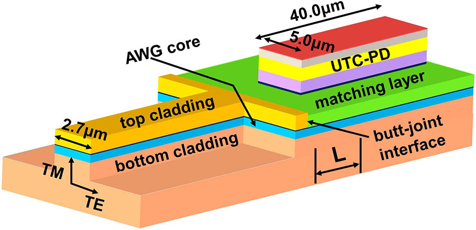
    Fig. 1. Butt-joint situation of AWG-UTC chip.
    Butt-joint (a) with and (b) without the extended matching layer.
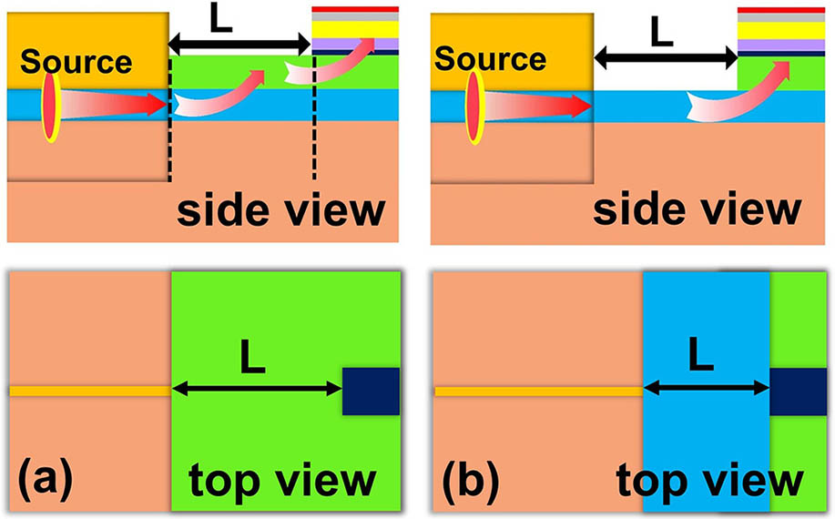
    Fig. 2. Butt-joint (a) with and (b) without the extended matching layer.
    (Color online) Simulated quantum efficiency of the PD with increasing distance between the butt-joint interface and the PD mesa.
    Fig. 3. (Color online) Simulated quantum efficiency of the PD with increasing distance between the butt-joint interface and the PD mesa.
    SEMs in device fabrication with (a): the butt-joint interface after SAG; (b): the overgrown ridge at the interface; (c): deep-ridge etched arrayed waveguides; (d): the PD after the AWG is cleaved off.
    Fig. 4. SEMs in device fabrication with (a): the butt-joint interface after SAG; (b): the overgrown ridge at the interface; (c): deep-ridge etched arrayed waveguides; (d): the PD after the AWG is cleaved off.
    Top views of the (a) 20 nm and (b) 800 GHz channel spacing AWG-UTC chips.
    Fig. 5. Top views of the (a) 20 nm and (b) 800 GHz channel spacing AWG-UTC chips.
    (Color online) Spectral photoresponse of the 20 nm channel spacing AWG-UTC chip.
    Fig. 6. (Color online) Spectral photoresponse of the 20 nm channel spacing AWG-UTC chip.
    (Color online) Spectral photo-response of the 800 GHz channel spacing AWG-UTC chip.
    Fig. 7. (Color online) Spectral photo-response of the 800 GHz channel spacing AWG-UTC chip.
    (Color online) Photocurrents of the PDs without the AWG.
    Fig. 8. (Color online) Photocurrents of the PDs without the AWG.
    (Color online) Bandwidth results for the AWG-UTC chips.
    Fig. 9. (Color online) Bandwidth results for the AWG-UTC chips.
    CompositionThickness (nm)Dopingn@1310 nmFunction
    In0.53Ga0.47As30P+3.65-i0.148p-contact
    InP300P+3.21Electron blocker
    In0.53Ga0.47As590P, graded3.65-i0.148Absorber
    InGaAsP (Q1.24)40N3.42Cliff layer
    InGaAsP (Q1.24)430U.I.D3.42Collector
    InP100N3.21Dopant blocker
    InGaAsP (Q1.24)500N+3.42Matching layer
    InP150U.I.D3.21Etch stop
    InGaAsP (Q1.05)500U.I.D3.298AWG core
    InP1000U.I.D3.21Bottom cladding
    Table 1. Epitaxial Structure Before Regrowth.
    Han Ye, Qin Han, Qianqian Lv, Pan Pan, Junming An, Xiaohong Yang, Yubing Wang, Rongrui Liu. 4×25GHz uni-traveling carrier photodiode arrays monolithic with InP-based AWG demultiplexers using the selective area growth technique[J]. Chinese Optics Letters, 2017, 15(8): 082301
    Download Citation