• Advanced Photonics Nexus
  • Vol. 2, Issue 2, 026007 (2023)
Haiyang Liu1、2, Zongnan Zhang1, Yingqiu Li1, Yaping Wu1、*, Zhiming Wu1、*, Xu Li1, Chunmiao Zhang1, Feiya Xu1, and Junyong Kang1
Author Affiliations
  • 1Xiamen University, Engineering Research Centre for Micro-Nano Optoelectronic Materials and Devices at Education Ministry, Fujian Provincial Key Laboratory of Semiconductor Materials and Applications, Department of Physics, Xiamen, China
  • 2Nanyang Technological University, School of Electrical and Electronic Engineering, Singapore
  • show less
    DOI: 10.1117/1.APN.2.2.026007 Cite this Article Set citation alerts
    Haiyang Liu, Zongnan Zhang, Yingqiu Li, Yaping Wu, Zhiming Wu, Xu Li, Chunmiao Zhang, Feiya Xu, Junyong Kang. Controllable valley magnetic response in phase-transformed tungsten diselenide[J]. Advanced Photonics Nexus, 2023, 2(2): 026007 Copy Citation Text show less
    (a) Optical topography of the CVD-grown large-scale WSe2 monolayer on SiO2/Si surface, where the tweezer trace shows the distinction between WSe2 film and the substrate. (b), (c) HRTEM image and SAED pattern of monolayer H/T-WSe2. (d) XPS of monolayer H/T-WSe2. The blue and purple shadows correspond to the components of H and T phases, respectively. (e) I–V curves of monolayer H-WSe2 and H/T-WSe2 with the T-phase components of 12.2% and 19.9%. (f) Atomic structure of monolayer H/T-WSe2, and the differential charge densities of top Se, W, and bottom Se atomic layers. The scale bar from blue to red denotes the change from depletion to accumulation.
    Fig. 1. (a) Optical topography of the CVD-grown large-scale WSe2 monolayer on SiO2/Si surface, where the tweezer trace shows the distinction between WSe2 film and the substrate. (b), (c) HRTEM image and SAED pattern of monolayer H/T-WSe2. (d) XPS of monolayer H/T-WSe2. The blue and purple shadows correspond to the components of H and T phases, respectively. (e) IV curves of monolayer H-WSe2 and H/T-WSe2 with the T-phase components of 12.2% and 19.9%. (f) Atomic structure of monolayer H/T-WSe2, and the differential charge densities of top Se, W, and bottom Se atomic layers. The scale bar from blue to red denotes the change from depletion to accumulation.
    Circularly polarized PL spectra of H/T-WSe2-19.9% under (a)–(d) positive magnetic fields from 1 to 4 T and (e)–(h) negative magnetic field from −1 to −4 T. The blue and purple lines indicate co- and cross-polarized configurations, respectively.
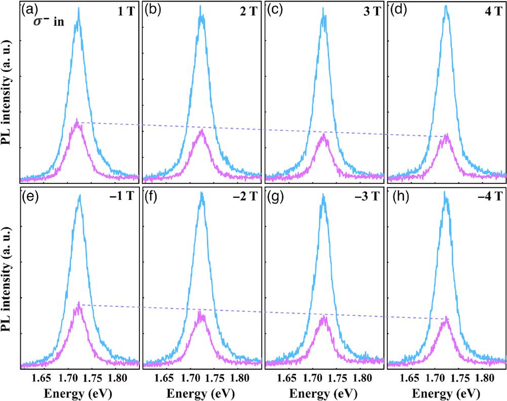
    Fig. 2. Circularly polarized PL spectra of H/T-WSe2-19.9% under (a)–(d) positive magnetic fields from 1 to 4 T and (e)–(h) negative magnetic field from 1 to −4 T. The blue and purple lines indicate co- and cross-polarized configurations, respectively.
    Magnetic-dependent polarization of (a) H/T-WSe2-12.2% and (b) H/T-WSe2-19.9% under σ− excitation with σ− and σ+ detection. The red dots indicate the measurement data. The dark blue, light blue, and pink lines show slopes from 0 to ±1 T, ±1 to ±2 T, and ±2 to ±4 T, respectively. Spin density isosurface plots of (c) H-WSe2 and (d) H/T-WSe2. The W and Se atoms are denoted by the blue and yellow balls, respectively. The isosurface in pink represents the majority spin density. Total spin DOSs of monolayers (e) H-WSe2 and (f) H/T-WSe2, where the pink and blue lines denote the majority and minority spin DOS.
    Fig. 3. Magnetic-dependent polarization of (a) H/T-WSe2-12.2% and (b) H/T-WSe2-19.9% under σ excitation with σ and σ+ detection. The red dots indicate the measurement data. The dark blue, light blue, and pink lines show slopes from 0 to ±1  T, ±1 to ±2  T, and ±2 to ±4  T, respectively. Spin density isosurface plots of (c) H-WSe2 and (d) H/T-WSe2. The W and Se atoms are denoted by the blue and yellow balls, respectively. The isosurface in pink represents the majority spin density. Total spin DOSs of monolayers (e) H-WSe2 and (f) H/T-WSe2, where the pink and blue lines denote the majority and minority spin DOS.
    Schematic diagram of magnetic-field-modulated valley dynamic process of monolayer H-WSe2 and H/T-WSe2. (a) SOC-induced valence band splitting in H-WSe2. (b) SOC induced band splitting in H/T-WSe2 with the electron concentration increases due to the introduction of T phase in H-WSe2. (c) Magnetic-field-induced exciton dispersion in conduction band and valley splitting in valence band of H/T-WSe2. (d) Cartoons depicting valley polarization in H/T-WSe2 under the (d) positive and (e) negative magnetic fields, respectively. The thick arrows with single color (γ1) denote the asymmetric valley-conserving and the thin arrows (γ2) with color gradient denote the valley-flipping exciton formation processes under σ+ and σ− excitation.
    Fig. 4. Schematic diagram of magnetic-field-modulated valley dynamic process of monolayer H-WSe2 and H/T-WSe2. (a) SOC-induced valence band splitting in H-WSe2. (b) SOC induced band splitting in H/T-WSe2 with the electron concentration increases due to the introduction of T phase in H-WSe2. (c) Magnetic-field-induced exciton dispersion in conduction band and valley splitting in valence band of H/T-WSe2. (d) Cartoons depicting valley polarization in H/T-WSe2 under the (d) positive and (e) negative magnetic fields, respectively. The thick arrows with single color (γ1) denote the asymmetric valley-conserving and the thin arrows (γ2) with color gradient denote the valley-flipping exciton formation processes under σ+ and σ excitation.
    Haiyang Liu, Zongnan Zhang, Yingqiu Li, Yaping Wu, Zhiming Wu, Xu Li, Chunmiao Zhang, Feiya Xu, Junyong Kang. Controllable valley magnetic response in phase-transformed tungsten diselenide[J]. Advanced Photonics Nexus, 2023, 2(2): 026007
    Download Citation