Carlo De Santi1、*, Matteo Meneghini1、4, Desiree Monti1, Johannes Glaab2, Martin Guttmann3, Jens Rass2, Sven Einfeldt2, Frank Mehnke3, Johannes Enslin3, Tim Wernicke3, Michael Kneissl2、3, Gaudenzio Meneghesso1, and Enrico Zanoni1
Carlo De Santi, Matteo Meneghini, Desiree Monti, Johannes Glaab, Martin Guttmann, Jens Rass, Sven Einfeldt, Frank Mehnke, Johannes Enslin, Tim Wernicke, Michael Kneissl, Gaudenzio Meneghesso, Enrico Zanoni. Recombination mechanisms and thermal droop in AlGaN-based UV-B LEDs[J]. Photonics Research, 2017, 5(2): A44
Copy Citation Text
This paper reports a comprehensive analysis of the origin of the electroluminescence (EL) peaks and of the thermal droop in UV-B AlGaN-based LEDs. By carrying out spectral measurements at several temperatures and currents, (i) we extract information on the physical origin of the various spectral bands, and (ii) we develop a novel closed-form model based on the Shockley–Read–Hall theory and on the ABC rate equation that is able to reproduce the experimental data on thermal droop caused by non-radiative recombination through deep levels. In the samples under test, the three EL bands are ascribed to the following processes: band-to-band recombination in the quantum wells (main EL peak), a parasitic intra-bandgap radiative transition in the quantum well barriers, and a second defect-related radiative process in the -AlGaN superlattice.
The UV-B spectral range, from 280 to 320 nm, is of great interest for several applications. Effective treatment of skin diseases [1], UV curing [2], and enhancement of plant growth [3] have already been demonstrated, but the conventional light sources in this spectral region are bulky, have limited lifetime, and contain toxic substances. For this reason, UV-B LEDs are promising devices, but their reliability still needs improvements [4]; in addition, the electroluminescence (EL) spectrum is often constituted by several emission bands that reduce the spectral purity.
Finally, the efficiency of UV-B LEDs is still low compared to their visible counterparts. This is partly due to the low light extraction efficiency of AlGaN-based structures [5] and partly to the non-radiative recombination losses [Shockley–Read–Hall (SRH) and Auger-related] that limit the internal quantum efficiency at low and high current levels. Recent papers indicated that the reduction in optical power with increasing temperature (referred to as thermal droop) may also limit the performance of GaN-based LEDs, causing an emission decrease comparable to the more discussed efficiency droop [6,7]. This is particularly relevant for UV LEDs, which—owing to the lower efficiency—convert most of the electrical power to heat. This effect is quantitatively ascribed to increased carrier escape or defect-related non-radiative recombination [8,9], but no comprehensive analysis or accurate theoretical model is present in the literature.
Understanding the physical origin of the parasitic peaks is important to reduce their contribution and improve the spectral purity of the devices. With the aim of obtaining more insight on these physical processes, within this paper we propose a new approach that has the following novelty elements: (i) the combined analysis of both spectral and temperature-dependent data, (ii) the definition of a closed-form model for the thermal droop caused by the SRH non-radiative recombination through deep levels—this model is based on the SRH theory and on the ABC rate equation, and (iii) a complete and consistent analysis of the various effects occurring in a wide temperature and bias current range.
Sign up for Photonics Research TOC. Get the latest issue of Photonics Research delivered right to you!Sign up now
2. EXPERIMENTAL DETAILS
The devices under test were grown by metal-organic vapor phase epitaxy on (0001) sapphire substrates. After a 700 nm thick AlN buffer layer, an AlN/GaN superlattice was introduced to relax the strain of an upper thick buffer and n-AlGaN current spreading layer. The active region is composed of three 2 nm thick nominally undoped quantum wells (QWs) separated by AlGaN barriers, giving a 308 nm nominal peak emission wavelength. The side of the structure employs a 25 nm -doped electron blocking layer (EBL), followed by a -doped AlGaN/AlGaN short-period superlattice (SPSL) and a thin -GaN contact layer. Additional details on the structure can be found in Refs. [10,11]. Subsequently, the wafers were fabricated into UVB-LED chips (junction area ) with standard processing techniques. The resulting devices show a nominal output power of 4.2 mW at 100 mA, which is in the range of typical current devices on the market. Details of the fabrication process can be found in Refs. [10,12].
To understand the origin of the EL and the role of the different thermal droop mechanisms, electrical and optical characteristics were measured in a liquid nitrogen cryostat from 100 to 400 K. The spectral power distribution of the EL was collected at five different currents, namely, 10 μA, 100 μA, 1 mA, 10 mA, and 100 mA, by means of a compact array spectrometer. The bias current was supplied by a precision parameter analyzer.
3. SPECTRAL ANALYSIS
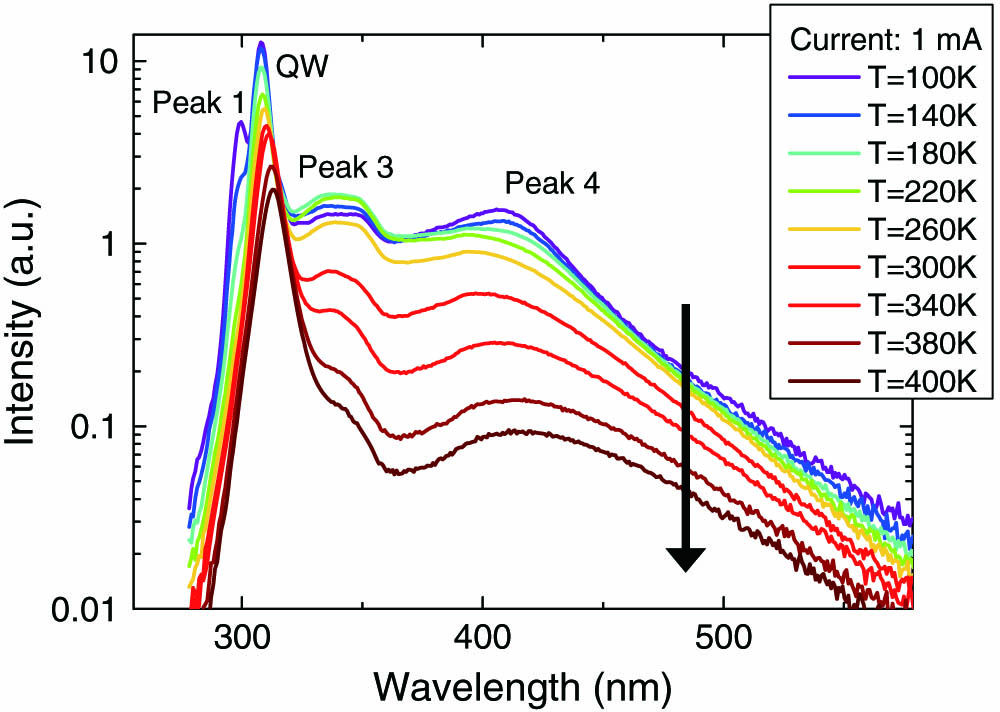
The EL spectra collected at the various test temperatures are reported in Fig. 1 exemplarily for the 1 mA bias current. Several different spectral features can be noticed, including four peaks, which are referred to as peak 1, QW, peak 3, and peak 4 in the following. Complex (multi-band) emission spectra from UV devices were already reported in the past [13–16]. The strongest parasitic emission peaks at 4% at room temperature, and this is comparable to state-of-the-art commercial devices with similar performances [17].
Figure 1.Spectral distribution of the EL at various temperatures and a current of 1 mA. The four main emission peaks are labeled in the figure.
The wavelength of the second peak (“QW”) is compatible with the nominal emission from the QWs. A detailed analysis on the effect of bias current and temperature will be given in the following sections, which will also discuss the origin and behavior of peaks 3 and 4.
Peak 1 is visible only at the lowest temperature and current levels and is not relevant for the room temperature performance of the devices. For this reason, its analysis is beyond the scope of this paper. The collected experimental data do not point out a clear origin of this peak, which will be analyzed by means of a specific set of tests in the future.
4. ANALYSIS OF THE QW LUMINESCENCE
The analysis of the QW emission peak as a function of temperature and measuring current is summarized in Fig. 2. Three different thermal droop regimes can be identified.
Figure 2.Intensity of the QW emission for different temperatures and currents.
The first one is visible at for the three lower currents (). In this case, a significant decrease in the optical power is detected even for small temperature variations; this effect is more prominent at low currents.
The temperature dependence of the optical power was fitted according to the well-known equation where is the extrapolated intensity at , a proportionality constant, the activation energy of the process causing the decrease in the optical power, and the Boltzmann constant [18]. The results reported in Fig. 3 show a very good quality of the fit and a low value of the activation energy of about 70 meV. This behavior can be explained by taking into account the exciton delocalization inside the QWs [19]. Electrons and holes may be localized in potential minima, caused by fluctuations in the alloy composition or in the QW thickness. When the temperature is increased, the carriers can gain enough energy to overcome the small potential barrier confining them in the localized states, thus becoming delocalized in the plane of the QWs. This lowers the probability of an electron–hole interaction and decreases the rate of radiative recombination [20–23]. This hypothesis is supported by the low activation energy derived in Fig. 3, which is comparable to values reported for exciton delocalization [24–27]. Typical reported values of localization potential in AlGaN are, in some cases, lower, but the average radius of the composition fluctuation was recently shown to have a strong impact on the localization potential [27]. Additionally, our devices have a small In content in the QWs, which was shown to potentially increase the localization energy [28].
Figure 3.Arrhenius plot of the intensity of the QW emission and fit according to Eq. (1).
An additional confirmation that for the reduction in optical power of the QW emission with increasing temperature is caused by exciton delocalization rather than by SRH recombination is given by the analysis of the peak wavelength of the QW emission shown in Fig. 4. The almost constant wavelength of the emission at low temperature (from 100 to 160 K) is not consistent with an increase in SRH recombination, which would add an additional redshift to the redshift of the bandgap in accordance with Varshni’s law due to the reduced density of carriers available for radiative recombination inside the QWs. Rather, the almost constant emission wavelength corresponds to a superimposed blueshift from localized electrons and holes that are thermally excited to higher energy states. At higher temperatures (), the peak wavelength strongly shifts red, caused by the bandgap narrowing with increasing temperature and confirmed by a fitting using Varshni’s law (see the inset in Fig. 4) [29].
Figure 4.Temperature dependence of the peak wavelength of the QW emission. Inset: bandgap narrowing with increasing temperature in accordance with Varshni’s law.
The second thermal droop regime is visible in Fig. 2 for for all currents. This can be clearly distinguished from the previous mechanism as a separate one due to the transition temperature range around 250–300 K. We propose SRH recombination as a good candidate for explaining such a decrease in the optical power.
Several reports [30–33] used Eq. (1) to analyze the decrease in optical power at high temperatures. This formula is effective to investigate the thermal droop due to exciton delocalization, but it is not adequate to study the impact of SRH recombination (even if it is used sometimes in the literature [34–36]). In fact, it can be noticed from Eq. (2) that the optical power does not approach zero for infinitely high temperatures, whereas we expect this trend when the temperature increases significantly [21,37–39]:
Equation (1) is a simplification, as is clear from the theoretical background described, for example, in Ref. [40]. First, the distribution of the carriers is approximated by the Boltzmann distribution rather than described by the Fermi distribution. Moreover, the defect density, which acts as a rate-limiting element in the SRH recombination process, is not taken into account. An additional problem may arise from the assumption that the number of excitons in the QWs does not depend on temperature, which may not be reasonable over a wide temperature range due to additional temperature-dependent loss mechanisms (such as carrier escape, thermionic emission, and injection efficiency). Finally, Eq. (1) does not take into account the particular expressions of the capture and emission rates typical of the SRH process.
For this reason, we followed a novel approach based on the ABC rate equation [41,42] and on the approximated formula for the SRH non-radiative recombination lifetime : where is a constant that depends on the deep level density and on the carrier capture rate, is the trap energy level, and the intrinsic Fermi energy level [43]. According to the ABC model and assuming perfect injection efficiency, the rate equation of an LED can be written as
Here, is the electron electrical charge, the recombination volume, the SRH recombination coefficient, the bimolecular radiative recombination coefficient, the Auger recombination coefficient, and the carrier concentration. The internal quantum efficiency can then be expressed as
Based on Eqs. (3)–(5), it is possible to develop an analytical model for the thermal droop. When taking two temperatures , the variation in internal quantum efficiency is where the subscript number in , , , and is a reference to the corresponding temperature value. Under the assumption that the value of is not temperature dependent and that the Auger recombination is negligible (no efficiency droop was detected up to 30 mA), Eq. (6) can be rewritten as
If the current at the two temperatures is the same, and assuming that the recombination volume does not vary with temperature, we obtain from Eq. (4) and therefore where only the positive solution was kept, because the carrier concentration cannot be negative.
By using Eqs. (3), (7), and (9), it is possible to fit the experimental data for every current. The results shown in Fig. 5 demonstrate a good agreement between theory and experiment. To achieve the best fitting quality, the parameters , , , , and had to be fitted independently for each current (but are kept constant, when not explicitly stated, for every temperature), which may partly result from the simplicity of the model. The increase in the density of carriers at different bias levels is expected, and the variation in the recombination coefficients is consistent with several reports [41,44–48]. The parameters remained within a reasonable range, if the variation of the parameters with current density mentioned above is taken into account [44] (e.g., from to , from to ), when compared to data available for InGaN-based devices [41,49] (given the lack of experimental reports on these values for AlGaN LEDs), confirming that the model achieves good fitting quality with meaningful parameters, comparable to experimental ones. The fitting indicated that the deep levels responsible for SRH recombination are located close to mid-gap ( in the range between 165 and 342 meV). Therefore, we conclude that above 300 K (i.e., at realistic temperatures of device operation), the thermal droop is caused by the increased SRH recombination.
Figure 5.Intensity of the QW emission for different temperatures and currents fitted by Eqs. (3), (7), and (9).
The third region of interest in Fig. 2 is the part at low temperature () and high current (). In this case, the optical power emitted by the QW increases (instead of decreasing) with increasing temperature. This effect can be related to an enhanced hole injection from the side to the QWs, as previously proposed for similar samples [10,11]. The enhanced hole injection at higher temperature is confirmed by numerical simulations based on a one-dimensional drift-diffusion model of the band structure and carrier concentration [50], as shown in Fig. 6. Here, the temperature dependence of the bandgap is described by Varshni’s empirical expression, and the charge carrier mobility is set constant in the temperature range. When the temperature is increased from 140 to 300 K, the electron concentration in the QWs is not expected to vary significantly, but the hole concentration in the farthest QW is expected to increase. The higher hole density causes the detected increase in optical power.
Figure 6.Numerical simulation of the band diagram and of electron and hole concentration at 140 and 300 K at a current of 10 mA.
The presence of excitons and excitonic recombination has been shown to play an important role in time-resolved photoluminescence (TRPL) studies, even at high temperature and high excitation densities [51,52]. As reported in Ref. [52], the exciton density rapidly decreases in hundreds of picoseconds (even without self-heating), more rapidly than the e-h plasma. Both studies analyze TRPL with (at most) picosecond-long laser pulses, and there is no evidence that this process would impact the longer timescale of CW operation (the condition of our thermal droop analysis), especially if the self-heating of the device is taken into account. Even if we assume that excitons are present, their very low binding energy (50 meV at most, according to Refs. [51,52]) would lead to a significant dissociation in the long term, due to multi-phonon processes and to the energy distribution of the phonons. During a capacitance deep level transient spectroscopy experiment, it is possible to detect, at room temperature, thermal emission from deep levels about 0.6–0.8 eV below the conduction band and about 0.2–0.3 eV at 100 K [53–58]. For all these reasons, excitonic effects are probably negligible in our thermal droop analysis.
5. PEAK 3 ANALYSIS
The EL intensity of peak 3 as a function of temperature and current is summarized in Fig. 7. In this case, at low currents we do not observe the double-slope behavior highlighted in Fig. 2 for the QW peak. The analysis of the thermal droop reveals that the intensity of peak 3 can also be fitted according to the complete SRH model based on Eqs. (3), (7), and (9). For this reason, non-radiative recombination through deep levels inside the bandgap is the likely cause for the reduction in the optical power of peak 3 with increasing temperature.
Figure 7.Arrhenius plot of the peak 3 intensity for different currents fitted by the complete SRH model [Eqs. (3), (7), and (9)].
Information on the physical origin of peak 3 was obtained by the behavior at low temperature for the three highest currents. As can be noticed in Fig. 7, the optical power increases with increasing temperature, as already found for the QW peak. Therefore, peak 3 is also affected by the hole injection efficiency, and the layer responsible for this EL has to be located beyond the side of the device. By using this information and by comparing the peak emission wavelength with the nominal bandgap values of the different layers in the heterostructure, we suggest that peak 3 originates from radiative transitions through deep levels, as confirmed by the broad shape of the peak (see Fig. 1), which is a common signature of parasitic intra-gap emission. This radiative recombination is most probably occurring in the quantum barrier next to the EBL and not inside the QWs, because no effect of exciton delocalization is detected, whereas it is present for the main QW peak. This hypothesis is supported when multiplying the hole and electron concentration shown in Fig. 6, because this product is directly proportional to the recombination rate. The results of the product show (not shown in this paper), besides strong peaks within the QWs, an increased value in that part of the band structure.
6. ANALYSIS OF PEAK 4
The analysis of the origin of peak 4 and of its thermal droop is more complex than for the other peaks. In this case, the SRH model does not fit the experimental data adequately (see Fig. 8 for three representative current values). For this reason, we suggest that a different mechanism may play an important role. The first information originates from the behavior at low temperature: contrary to the QW peak and peak 3, no increase in the optical power is detected with increasing temperature, suggesting that this emission process is not limited by hole injection and, therefore, that its source is probably located in the side. Comparing the wavelength of peak 4 with the layer structure of the side as well as considering the spectral width of peak 4 (see Fig. 1) suggests that peak 4 is likely related to a radiative parasitic transition inside the region with the lowest energy gap in the side, i.e., the AlGaN/AlGaN SPSL, where the density of holes available for the emission is highest.
Figure 8.Arrhenius plot of the peak 4 intensity for different currents fitted by the complete SRH model [Eq. (7)].
These assumptions can be supported by again analyzing the simulation results of the band structure, carrier densities, and recombination rates as partially shown in Fig. 6. Taking the radiative recombination rate in the superlattice for different temperatures, a similar dependence can be recognized, as it is observed in the normalized intensity of peak 4 as a function of shown in Fig. 8. It should be noted, however, that the simulation does not take into account hole injection mechanisms at the contact and, therefore, only partially reflects the experiment. The simulation shows that at low temperatures the band bending in the EBL is lower, because fewer acceptors are ionized and a higher external voltage is needed to maintain the current flow (mainly electrons at low temperature). Thus, more electrons overcome the EBL, penetrate into the side, and recombine radiatively there. At higher temperatures more acceptors are ionized, a lower voltage is needed to inject holes in the active region, and, hence, the EBL works more efficiently preventing electron leakage into the side.
The presence of various radiative transitions in the side was already reported in the past, and qualitatively ascribed to several origins, such as band-to-band recombination promoted by defect-assisted electron tunneling [8] and radiative recombination through deep acceptor levels [59,60] or complexes [16].
An extended analysis of the temperature dependence of peak 4 becomes even more complex if the temperature and current dependence of the electron leakage across the EBL is taken into account. Additionally, the broad peak 4 may be the composition of several defect-related radiative recombination channels, given the asymmetric shape of peak 4 (see Fig. 1). All these aspects prevent a clear identification of the physical mechanism of the thermal droop. Given the short periodicity of the superlattice, it could also include field- or trap-assisted escape processes, such as phonon-assisted tunneling, trap-assisted tunneling, or more accurate models [6].
7. CONCLUSIONS
In summary, in this paper we showed that the temperature and current dependence of AlGaN UV-B LEDs can provide useful information on the physical origin of multiple EL peaks. Moreover, we developed a new closed-form model based on the SRH recombination lifetime and on the ABC model that can be used to closely fit the decrease of the optical power with increasing temperature caused by the non-radiative recombination through deep levels.
With increasing temperature, the QW emission showed three different trends that have been investigated in detail. At low temperature and high currents an increase in the optical power, caused by an enhanced hole injection from the side to the side, was found. At high temperature, the optical power is reduced due to a more common increase in the SRH recombination rate, whereas at low temperature and low current, the reduction is likely caused by exciton delocalization from potential minima inside the QWs.
A second emission peak (peak 3) originates most likely from parasitic intra-bandgap radiative transitions beyond the side of the device and is influenced by the enhanced hole injection with increasing temperature at high currents. A possible location is in the quantum barrier next to the EBL, because we have not detected any exciton delocalization effect.
The third emission peak (peak 4) is the most complex one. It is attributed to a parasitic radiative transition, possibly in the -AlGaN superlattice and assisted by a charge transfer mechanism.
Acknowledgment
Acknowledgment. The authors would like to thank the materials technology department and the process technology department at the Ferdinand-Braun-Institut for their contributions in the development of the UV-B LEDs. This work was partially supported by the German Federal Ministry of Education and Research through the consortia project “Advanced UV for Life.” Further support was given by the Federal Ministry for Economic Affairs and Energy through the project “UV-Berlin” as well as by the Deutsche Forschungsgemeinschaft within the Collaborative Research Center “Semiconductor NanoPhotonics.”
APPENDIX A: SIMPLIFIED SRH MODEL
The fitting algorithm based on Eqs. (3), (7), and (9) is complex and requires some computation time. The model can be simplified considering that for the carrier concentration is slightly lower than (due to the increased SRH recombination), and we can write this difference as
By using Eq. (A1) in Eq. (7), we obtain
If the variation in carrier concentration between two subsequent temperature points is small , Eq. (A2) can be approximated as
By using Eq. (A3) instead of Eq. (7) together with Eqs. (3) and (9), we can obtain a simpler and quicker fitting algorithm. As can be noticed in Fig. 9 for the representative current of 10 mA, the fitting quality obtained by using the approximated Eq. (A3) (red line) is lower than the more accurate Eq. (7) (blue line), but agreement is still acceptable.
Figure 9.Intensity of the QW emission at different temperatures fitted by the complete SRH model [Eq. (7)] and the approximated model [Eq. (A3)], respectively.
Carlo De Santi, Matteo Meneghini, Desiree Monti, Johannes Glaab, Martin Guttmann, Jens Rass, Sven Einfeldt, Frank Mehnke, Johannes Enslin, Tim Wernicke, Michael Kneissl, Gaudenzio Meneghesso, Enrico Zanoni. Recombination mechanisms and thermal droop in AlGaN-based UV-B LEDs[J]. Photonics Research, 2017, 5(2): A44