• Journal of Semiconductors
  • Vol. 43, Issue 3, 034102 (2022)
Wensi Cai, Haiyun Li, Mengchao Li, and Zhigang Zang
Author Affiliations
  • Key Laboratory of Optoelectronic Technology & System (Ministry of Education), Chongqing University, Chongqing 400044, China
  • show less
    DOI: 10.1088/1674-4926/43/3/034102 Cite this Article
    Wensi Cai, Haiyun Li, Mengchao Li, Zhigang Zang. Performance enhancement of solution-processed InZnO thin-film transistors by Al doping and surface passivation[J]. Journal of Semiconductors, 2022, 43(3): 034102 Copy Citation Text show less
    (Color online) (a) Hall mobility and carrier concentration of the IZO:Al films. (b) Absorbance and corresponding bandgap (inset) of the IZO:Al films. Surface morphology of IZO films doped with (c) 0%, (d) 1%, (e) 3% and (f) 5% Al.
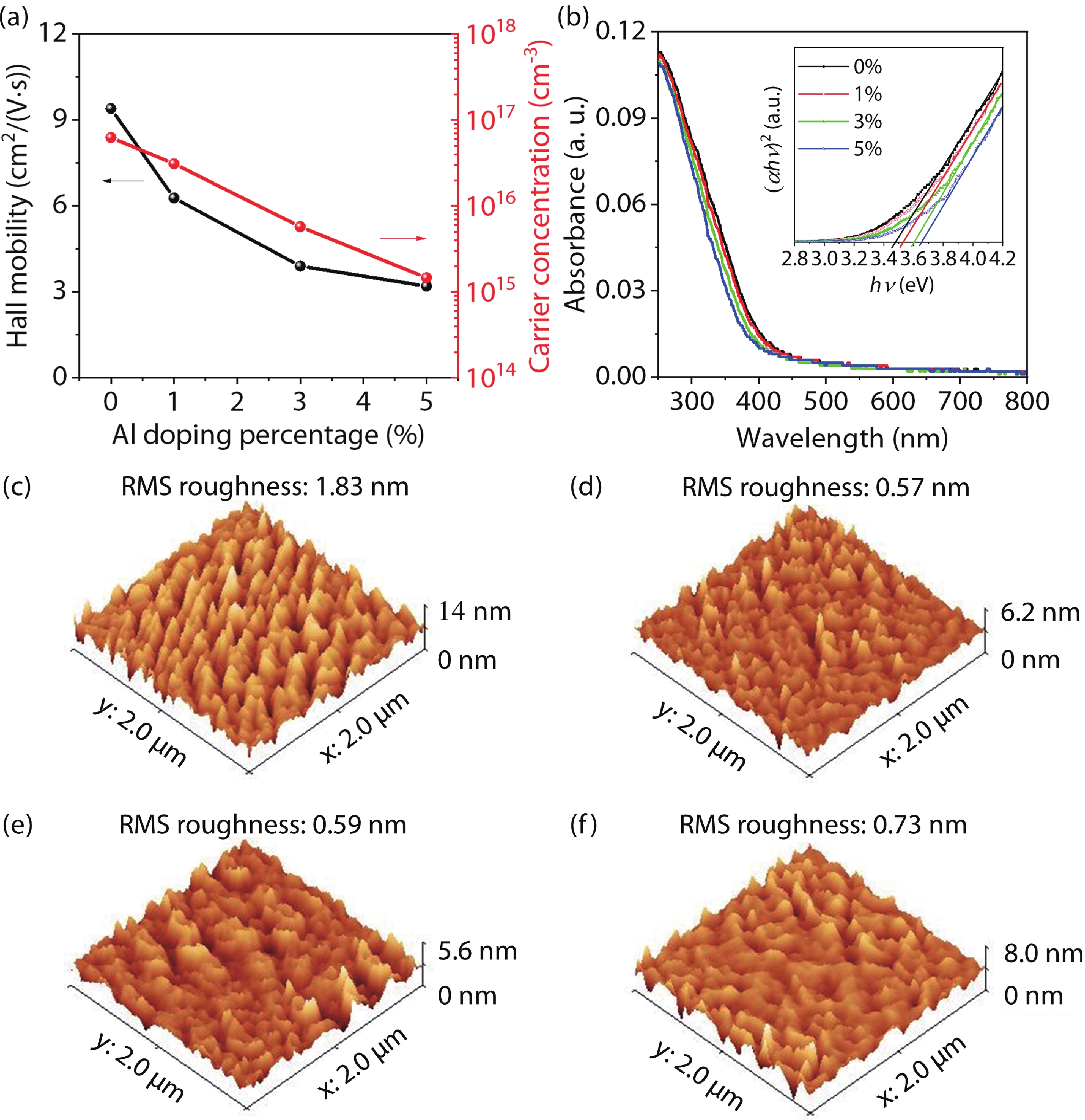
    Fig. 1. (Color online) (a) Hall mobility and carrier concentration of the IZO:Al films. (b) Absorbance and corresponding bandgap (inset) of the IZO:Al films. Surface morphology of IZO films doped with (c) 0%, (d) 1%, (e) 3% and (f) 5% Al.
    (Color online) O 1s spectra of IZO:Al films doped with (a) 0%, (b) 1%, (c) 3% and (d) 5% Al.
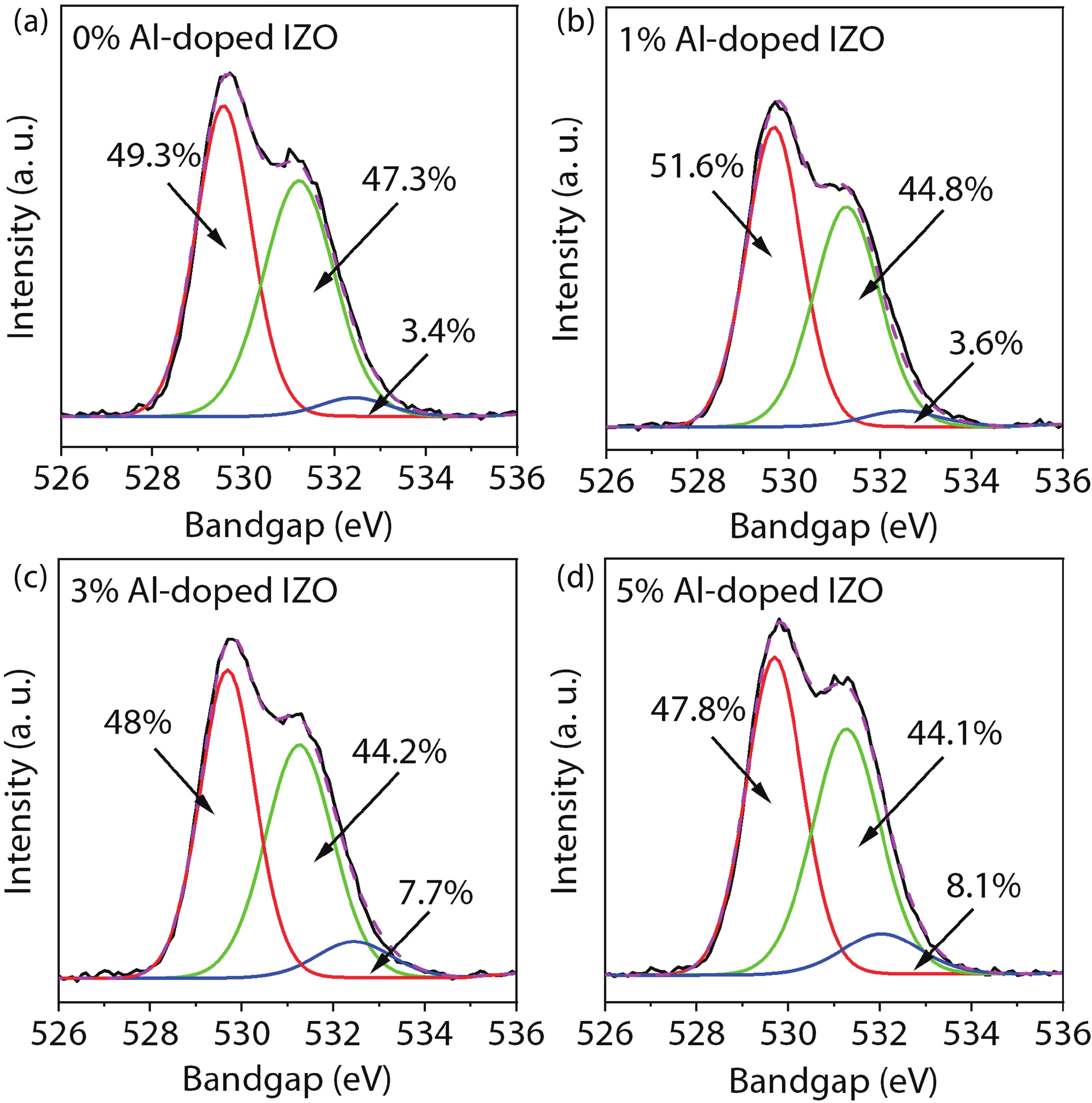
    Fig. 2. (Color online) O 1s spectra of IZO:Al films doped with (a) 0%, (b) 1%, (c) 3% and (d) 5% Al.
    (Color online) Transfer characteristics of IZO:Al TFTs (a) without and (b) with an OTES top surface treatment. The insets show images of a water drop on the surface of the IZO:Al films. (c) Schematic diagrams of TFT structures and OTES formation on IZO:Al surface. R represents C18H37.
    Fig. 3. (Color online) Transfer characteristics of IZO:Al TFTs (a) without and (b) with an OTES top surface treatment. The insets show images of a water drop on the surface of the IZO:Al films. (c) Schematic diagrams of TFT structures and OTES formation on IZO:Al surface. R represents C18H37.
    (Color online) Threshold voltage shift of IZO:Al TFTs under (a) a positive bias stress (PBS) and (b) a negative bias stress (NBS). Transfer characteristics of (c) 0% and (d) 1% Al doped IZO TFTs before and after being stored in ambient air for 4 months.
    Fig. 4. (Color online) Threshold voltage shift of IZO:Al TFTs under (a) a positive bias stress (PBS) and (b) a negative bias stress (NBS). Transfer characteristics of (c) 0% and (d) 1% Al doped IZO TFTs before and after being stored in ambient air for 4 months.
    (Color online) (a) Current density as a function of applied voltage for Si/AlOx/Al capacitors. (b) Surface morphology of AlOx. (c) Output and (d) transfer characteristics of low-voltage IZO:Al TFTs.
    Fig. 5. (Color online) (a) Current density as a function of applied voltage for Si/AlOx/Al capacitors. (b) Surface morphology of AlOx. (c) Output and (d) transfer characteristics of low-voltage IZO:Al TFTs.
    Al doping percentageTreatment or notCurrent on/off ratio (106) VTH (V) SS (V/dec)μ (cm2/(V·s)) Dtotal (1012 cm–2 eV–1)
    0%No3.85.670.723.92.38
    Yes4.15.50.615.61.98
    1%No86.60.643.52.09
    Yes106.350.574.21.84
    3%No4.810.20.691.782.27
    Yes4.87.970.591.871.91
    5%No3.912.720.690.812.27
    Yes4.39.240.61.321.95
    Table 1. Electrical properties of IZO:Al TFTs.
    μ (cm2/(V·s)) VG range (V) VON (V) ION/IOFFVTH (V) SS (V/dec) Dtotal(1012 cm–2eV–1) Ref.
    4.6–0.5 to 1.5–0.081.4 × 1040.50.171.6This work
    0.06–0.5 to 1–0.3>1050.20.08512[33]
    0.15–0.5 to 1–0.25~1040.0013//[35]
    3.2–1 to 20.18106/0.073/[36]
    7.23–1 to 303.06 × 1061.32//[37]
    13.4–1 to 3–0.7>1050.44//[38]
    1.05–5 to 50.21070.180.105/[39]
    5.48–2 to 6/1070.720.339[40]
    Table 2. Electrical performance of low-voltage, solution-processed oxide TFTs.
    Wensi Cai, Haiyun Li, Mengchao Li, Zhigang Zang. Performance enhancement of solution-processed InZnO thin-film transistors by Al doping and surface passivation[J]. Journal of Semiconductors, 2022, 43(3): 034102
    Download Citation