
Wensi Cai, Haiyun Li, Mengchao Li, Zhigang Zang. Performance enhancement of solution-processed InZnO thin-film transistors by Al doping and surface passivation[J]. Journal of Semiconductors, 2022, 43(3): 034102
- Journal of Semiconductors
- Vol. 43, Issue 3, 034102 (2022)
Abstract
1. Introduction
Ever since the first report of amorphous InGaZnO (IGZO) thin-film transistors (TFTs) in 2004 by Hosono et al. amorphous oxide semiconductors have received much attention owing to their excellent electrical properties[
InZnO (IZO) is considered as a promising n-type oxide semiconductor since it can be easily deposited through a solution process while maintaining a relatively high mobility under amorphous states. We have previously reported that by modifying the annealing temperature of solution-processed IZO TFTs, it is able to achieve a high mobility approaching 10 cm2/(V·s) and a high current on/off ratio[
Also, unlike Si and organic semiconductors, the top channel surface of oxide TFTs is extremely sensitive to air with water and -OH species being easily adsorbed on the top surface, resulting in a degraded device performance, particularly for those with an ultra-thin channel layer[
In this work, we explored the possibility of the performance enhancement in solution-processed IZO TFTs by doping and surface passivation. Electrical, optoelectronic and physical properties of TFTs were systematically studied in order to analysis the mechanism of Al doping and octadecyltrimethoxysilane (OTES) SAM top surface passivation. Due to reduced traps within the films and at the top surface, a significantly enhanced device performance was achieved, including an increased current on/off ratio, a reduced hysteresis and, most importantly, an improved bias stress stability. The combination of this optimized IZO:Al with high capacitance AlOx also enabled the demonstration of low-voltage TFTs, showing a mobility of 4.6 cm2/(V·s) and a current on/off ratio of > 10 4. The work might have potential implications in future high-performance, low-cost optoelectronic devices such as transparent displays.
2. Experimental procedures
2.1. Solutions
To prepare Al-doped IZO precursors, first, aluminium nitrate nonhydrate (Al(NO3)3·9H2O, 99.997%, Sigma), indium nitrate hydrate (In(NO3)3·xH2O, 99.99% Sigma), zinc nitrate hydrate (Zn(NO3)2·xH2O, 99.999%, Sigma) were separately dissolved in 2-Methoxyethanol (2-ME, 99%, Adamas) to yield solutions with a concentration of 0.2 M and stirred at room temperature for 24 h. Then the solutions were mixed together at a volume ratio of 0 : 50 : 50, 1 : 49.5 : 49.5, 3 : 48.5 : 48.5 and 5 : 47.5 : 47.5 for Al(NO3)3 : In(NO3)3 : Zn(NO3)2, respectively. The mixed solutions were stirred at room temperature for another 24 h and filtrated through 0.22 μm PTFE hydrophilic filters before use.
SAM solutions with a molar concentration of 0.01 M were prepared by adding octadecyltrimethoxysilane (OTES, 90%, Sigma) into toluene.
AlOx precursors were prepared by dissolving Al(NO3)3·9H2O into 2-ME to yield solutions with a concentration of 0.3 M. The solution was then stirred at room temperature for 24 h and filtrated through 0.22 μm PTFE hydrophilic filters before use.
2.2. Device fabrication
Approximately 33 nm thick AlOx films were deposited by spinning the precursor solutions at 2000 rpm for 35 s, followed by an immediate annealing at 120 °C for 1 min and another 1 h annealing at 350 °C in air.
To fabricate Al-doped IZO TFTs, first, precursors with different Al doping percentages were spin-coated on 100 nm thick SiO2 or AlOx films at 3000 rpm for 30 s, followed by an immediate annealing at 120 °C for 1 min and another 1 h annealing at 350 °C in air. Similar to what were reported previously, an intermediate annealing was done here in order to remove the residual solvent and/or rearrange the constituent elements within the layer[
2.3. Measurement and characterization
The hall mobility and carrier concentration of the IZO:Al films were measured at room temperature using a PhysTech RH2035 Hall System. The absorbance of the films was measured using an UV-VIS-NIR Spectrophotometer (Shimadu UV-3600). X-ray photoelectron spectroscopy (XPS) of the films was measured on a Thermo ESCALAB 250 Xi with Al Kα emission at 1486.6 eV. The surface morphology of the film was measured using an Asylum Research atomic force microscope (AFM). The electrical performance of the devices was measured using a Keithley 4200SCS semiconductor analyzer.
The turn-on voltage, Von, of TFTs is defined as the gate voltage, VG, at which drain current, ID, starts to increase in the ID–VG plot. The threshold voltage, VTH, in the saturation region is extracted from the linear extrapolation of the value of VG when ID = 0 from ID1/2–VG plot[
3. Results and discussions
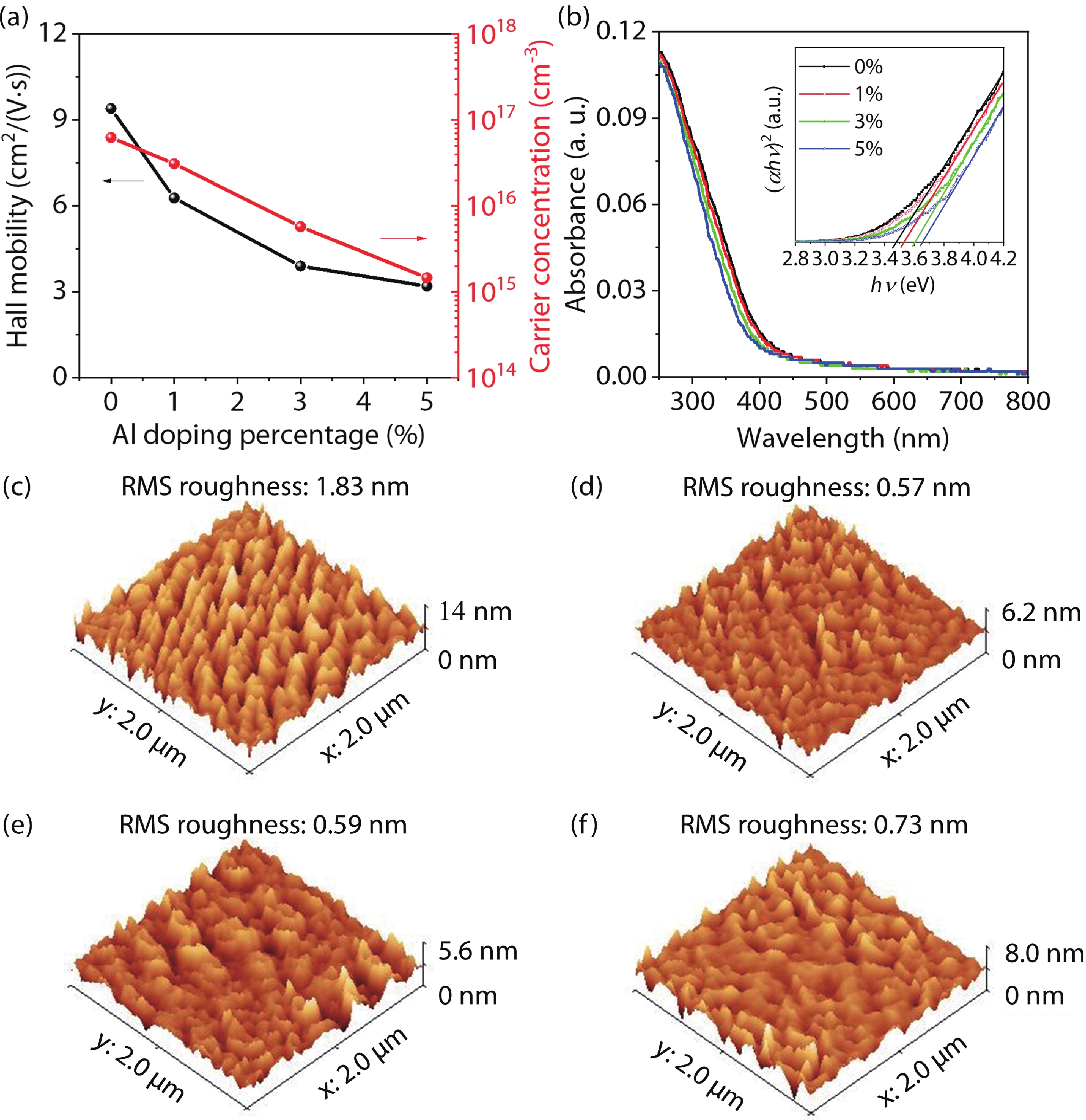
Fig. 1(a) shows the hall mobility as well as the carrier concentration of the IZO:Al films with different Al doping percentages. With the increase of Al addition from 0% to 5%, the hall mobility of the films drops from 9.4 to 3.2 cm2/(V·s), suggesting that the addition of Al into the IZO films suppresses the carrier generation and decreases the carrier concentration.
![]()
Figure 1.(Color online) (a) Hall mobility and carrier concentration of the IZO:Al films. (b) Absorbance and corresponding bandgap (inset) of the IZO:Al films. Surface morphology of IZO films doped with (c) 0%, (d) 1%, (e) 3% and (f) 5% Al.
The absorbance spectra of the IZO:Al films with different doping percentages are shown in Fig. 1(b), from which the bandgap of the films can be calculated using
where α is the optical absorption coefficient, h is the Planck’s constant, v is the frequency of light and Eg is the bandgap of the films. The inset of Fig. 1(b) shows the relationship between (αhv)2 and hv, from which bandgaps of 3.46, 3.52, 3.6, and 3.64 eV can be obtained for films doped with 0%, 1%, 3%, and 5% Al, respectively. An increase of bandgap is found here with the increase of Al doping percentages, suggesting a suppression of carrier concentration, which is in agreement with the results from Hall measurement.
The surface morphology of IZO:Al films is shown in Figs. 1(c)–1(f). The root-mean-square (RMS) roughness is found to be 1.83, 0.57, 0.59 and 0.73 nm for doping percentages of 0%, 1%, 3% and 5%, respectively. The doped films show a lower RMS roughness than undoped ones, which is attributed to the reduced trap states and surface modification by Al doping. With the films being amorphous for all the cases, the slight increase of RMS roughness at higher doping percentages might be caused by the aggregation of metal ions and generation of pinholes[
The XPS spectra of all films were then studied, as shown in Fig. 2 and Fig. S1. All films show In peaks at 444.2 and 451.8 eV, and Zn peaks at 1021.4 and 1044.3 eV (Fig. S1), demonstrating the existence of metal-oxide bonds[
![]()
Figure 2.(Color online) O 1s spectra of IZO:Al films doped with (a) 0%, (b) 1%, (c) 3% and (d) 5% Al.
To study the effects of Al doping on device performance, IZO:Al (0%, 1%, 3% and 5%) TFTs were fabricated, as shown in Fig. 3(a) and summarized in Table 1. With the increase of Al doping percentages from 0 to 5%, the transfer characteristics shift toward positive and the mobility decrease, which might be caused by the higher bonding energy of Al–O (5.31 eV/512.1 kJ/mol) than that of In–O (3.59 eV/346 kJ/mol) and Zn–O (2.94 eV/284.1 kJ/mol)[
![]()
Figure 3.(Color online) Transfer characteristics of IZO:Al TFTs (a) without and (b) with an OTES top surface treatment. The insets show images of a water drop on the surface of the IZO:Al films. (c) Schematic diagrams of TFT structures and OTES formation on IZO:Al surface. R represents C18H37.
Table Infomation Is Not Enablewhere k is the Boltzmann constant, T is the temperature, and q is the electron charge. Dtotal is 2.38 × 10¹², 2.09 × 10¹², 2.27 × 10¹² and 2.27 × 1012 cm–2eV–1 for TFTs doped with 0%, 1%, 3% and 5% Al, respectively. Lower Dtotal values are found in the doped TFTs, suggesting less traps existed at interface and/or within the film. The lowest Dtotal is found in TFTs doped with 1% Al, which is also in agreement with the film properties obtained from AFM and XPS measurements. Dtotal slightly increases at higher doping percentages (i.e., 3% and 5%), which might be due to the increase of scattering centres caused by the excess Al source and/or the creation of Al(OH)3[
In general, some water molecules from air might be easily adsorbed on the top channel surface of an oxide TFT and capture free electrons in the film through 2H2O + O2 + 4e– → 4OH–, resulting in a hydroxylated surface[
To test the effectiveness and reliability of Al doping and OTES treatment under operating conditions, bias stress stability of all TFTs were then studied, as shown in Figs. 4(a), 4(b), S2 and S3. While the devices without treatment show a large threshold voltage change of +4.58 V even only being positively biased at VG = 30 V for 600 s (Fig. S2(a)), the threshold voltage change dramatically reduces after the treatment (Fig. S2(b)). Such an improvement is considered mainly due to the reduction of top surface traps, as water exposure could significantly increase the bias stress instability of TFTs[
![]()
Figure 4.(Color online) Threshold voltage shift of IZO:Al TFTs under (a) a positive bias stress (PBS) and (b) a negative bias stress (NBS). Transfer characteristics of (c) 0% and (d) 1% Al doped IZO TFTs before and after being stored in ambient air for 4 months.
The results clearly suggest that the optimized condition is obtained at a doping percentage of 1%. We therefore study the long-term stability of 0% and 1% Al doped IZO TFTs, as shown in Figs. 4(c) and 4(d). Both TFTs show a reasonably good long-term stability, with fairly small changes of device performance even after being stored in ambient air for 4 months. Nevertheless, a smaller change is found in 1% doped case, with a threshold voltage change of only +0.11 V after the 4 months’ storage as compared to a change of +0.97 V for the undoped case. Such an improvement in the long-term stability is considered as the result of the improved film properties and/or the reduced trap states at the dielectric/channel interface due to doping since the doped TFTs show a lower total trap density.
For battery-powered portable electronics, a lower operating voltage could give a lower power consumption and hence a longer time of use without recharging. However, until now it is still quite challenging to achieve oxide TFTs with both a reasonably high current on/off ratio and a low operating voltage. Besides, the increasing need on printable electronics has led the attention on fully solution-processed TFTs. However, compared with their vacuum-deposited counterparts, solution-processed oxide TFTs generally show a poorer device performance, especially under a low operating voltage. To lower the operating voltage, here solution-processed AlOx films are used, which have a high gate capacitance of 143 nF/cm2. With a thickness of 32.95 ± 0.11 nm being measured for the film, this corresponds to a dielectric constant of 5.32. Such a value is lower than the theoretical value of Al2O3, which might be due to the formation of highly polar Al(OH)3 in the film[
![]()
Figure 5.(Color online) (a) Current density as a function of applied voltage for Si/AlO
With the use of such AlOx layers and 1% Al-doped IZO films, solution-processed IZO:Al TFTs were then demonstrated. The output characteristics in Fig. 5(c) suggest that the TFTs work in an n-type enhancement mode with linear, pinch-off and saturation regions clearly seen. The corresponding transfer characteristics are shown in Fig. 5(d). Owing to the high gate capacitance of AlOx, the TFTs show a low operating voltage of 1.5 V with a current on/off ratio of > 10 4, a mobility of 4.6 cm2/(V·s) and a subthreshold swing of 0.17 V/dec. The devices also show a turn-on voltage very close to 0 V with a negligible hysteresis between forward and backward sweeps, which is promising for circuit applications. A total trap density of 1.6 × 1012 cm–2eV–1 is calculated, which is either comparable to or even better than those with similar interfaces reported previously[
4. Conclusion
In conclusion, we studied the influence of Al addition and OTES treatment on the electrical, optoelectronic and physical properties of solution-processed IZO TFTs. Compared with pure IZO TFTs, optimized IZO:Al TFTs exhibited a significantly enhanced electrical performance, including an increase of current on/off ratio by a factor of 2.6 and a reduction of trap density by more than 23%. Such a hugely reduced trap density also dramatically improved the bias stress stability. Fully solution-processed IZO:Al TFTs were demonstrated, showing a low operating voltage of 1.5 V, a current on/off ratio of > 10 4, and a mobility of 4.6 cm2/(V·s). The reported work demonstrates a convenient and yet effective method to substantially improve the performance of solution-processed oxide TFTs, which might have potential applications in future low-cost, low-power printable electronics.
Acknowledgements
We thank the National Natural Science Foundation of China (11974063), China Postdoctoral Science Foundation (2020M683242), and Chongqing Special Postdoctoral Science Foundation (cstc2020jcyj-bshX0123) for financial support.
Appendix A. Supplementary material
Supplementary data associated with this article can be found, in the online version, at https: //doi.org/10.1088/1674-4926/43/3/034102.
References
[1] K Nomura, H Ohta, A Takagi et al. Room-temperature fabrication of transparent flexible thin-film transistors using amorphous oxide semiconductors. Nature, 432, 488(2004).
[2] E Fortunato, P Barquinha, R Martins. Oxide semiconductor thin-film transistors: a review of recent advances. Adv Mater, 24, 2945(2012).
[3] J W Park, B H Kang, H J Kim. A review of low-temperature solution-processed metal oxide thin-film transistors for flexible electronics. Adv Funct Mater, 30, 1904632(2020).
[4] W Cai, H Li, Z Zang. One-volt, solution-processed InZnO thin-film transistors. IEEE Electron Device Lett, 42, 525(2021).
[5] W J Park, H S Shin, B D Ahn et al. Investigation on doping dependency of solution-processed Ga-doped ZnO thin film transistor. Appl Phys Lett, 93, 083508(2008).
[6] D Y Zhong, J Li, Y H Zhou et al. The material properties of novel boron doped InZnO thin films by solution process and its application in thin film transistors with enhanced thermal stability. Superlattices Microstruct, 122, 377(2018).
[7] H J Jeon, W J Maeng, J S Park. Effect of Al concentration on the electrical characteristics of solution-processed Al doped ZnSnO thin film transistors. Ceram Int, 40, 8769(2014).
[8] A Reed, C Stone, K Roh et al. The role of third cation doping on phase stability, carrier transport and carrier suppression in amorphous oxide semiconductors. J Mater Chem C, 8, 13798(2020).
[9] W Cai, J Wilson, J Zhang et al. Significant performance enhancement of very thin InGaZnO thin-film transistors by a self-assembled monolayer treatment. ACS Appl Electron Mater, 2, 301(2020).
[10] W Cai, Z Zang, L Ding. Self-assembled monolayers enhance the performance of oxide thin-film transisotrs. J Semicond, 42, 030203(2021).
[11] W Zhong, G Li, L Lan et al. InSnZnO thin-film transistors with vapor-phase self-assembled monolayer as passivation layer. IEEE Electron Device Lett, 39, 1680(2019).
[12] P K Nayak, M N Hedhili, D Cha et al. Impact of soft annealing on the performance of solution-processed amorphous zinc tin oxide thin-film transistors. ACS Appl Mater Interfaces, 5, 3587(2013).
[13] Y G Kim, T Kim, C Avis et al. Stable and high-performance indium oxide thin-film transistor by Ga doping. IEEE Trans Electron Devices, 63, 1078(2016).
[14] W Cai, J Wilson, A Song. Present status of electric-double-layer thin-film transistors and their applications. Flex Print Electron, 6, 043001(2021).
[15] D N Kim, D L Kim, G H Kim et al. The effect of La in InZnO systems for solution-processed amorphous oxide thin-film transistors. Appl Phys Lett, 97, 192105(2010).
[16] R N Bukke, J K Saha, N N Mude et al. Lanthanum doping in zinc oxide for highly reliable thin-film transistors on flexible substrates by spray pyrolysis. ACS Appl Mater Interfaces, 12, 35164(2020).
[17] J Choi, J Park, K H Lim et al. Photosensitivity of InZnO thin-film transistors using a solution process. Appl Phys Lett, 109, 132105(2016).
[18] K H Lee, J H Park, Y B Yoo et al. Effects of solution temperature on solution-processed high-performance metal oxide thin-film transistors. ACS Appl Mater Interfaces, 5, 2585(2013).
[19] D Zhong, J Li, C Zhao et al. Enhanced electrical performance and negative bias illumination stability of solution-processed InZnO thin-film transistor by boron addition. IEEE Trans Electron Devices, 65, 520(2018).
[20] J Li, C X Huang, Y Z Fu et al. Amorphous LaZnSnO thin films by a combustion solution process and application in thin film transistors. Electron Mater Lett, 12, 76(2016).
[21] C Yang, Y Li, J Li. Ab initio total energy study of ZnO adsorption on a sapphire (0001) surface. Phys Rev B, 70, 045413(2004).
[22] D Wang, J Jiang, M Furuta. Investigation of carrier generation mechanismin fluorine-doped n+-In–Ga–Zn–O for self-aligned thin-film transistors. J Display Technol, 12, 258(2016).
[23]
[24] W Xu, D Liu, H Wang et al. Facile passivation of solution-processed InZnO thin-film transistors by octadecylphosphonic acid self-assembled monolayers at room temperature. Appl Phys Lett, 104, 173504(2014).
[25] L Shao, K Nomura, T Kamiya et al. Operation characteristics of thin-film transistors using very thin amorphous In–Ga–Zn–O channels. Electrochem Solid St Lett, 14, H197(2011).
[26] M E Lopes, H L Gomes, M C R Medeiros et al. Gate-bias stress in amorphous oxide semiconductors thin-film transistors. Appl Phys Lett, 95, 063502(2009).
[27] J K Jeong, H Won Yang, J H Jeong et al. Origin of threshold voltage instability in indium-gallium-zinc oxide thin film transistors. Appl Phys Lett, 93, 123508(2008).
[28] Y Jeong, C Bae, D Kim et al. Bias-stress-stable solution-processed oxide thin film transistors. ACS Appl Mater Interfaces, 2, 611(2010).
[29] A Suresh, J F Muth. Bias stress stability of indium gallium zinc oxide channel based transparent thin film transistors. Appl Phys Lett, 92, 033502(2008).
[30] W S Choi, H Jo, M S Kwon et al. Control of electrical properties and gate bias stress stability in solution-processed a-IZO TFTs by Zr doping. Curr Appl Phys, 14, 1831(2014).
[31] W Cai, S Park, J Zhang et al. One-volt IGZO thin-film transistors with ultra-thin, solution-processed Al
[32] L Lan, J Peng. High-performance indium–gallium–zinc oxide thin-film transistors based on anodic aluminum oxide. IEEE Trans Electron Devices, 58, 1452(2011).
[33] A Mukherjee, V Ottapilakkal, S Sagar et al. Ultralow-voltage field-effect transistors using nanometer-thick transparent amorphous indium–gallium–zinc oxide films. ACS Appl Nano Mater, 4, 8050(2021).
[34] H Ning, S Zhou, W Cai et al. Fabrication of high-performance solution processed thin film transistors by introducing a buffer layer. Appl Surf Sci, 504, 144360(2020).
[35] J Ko, J Kim, S Y Park et al. Solution-processed amorphous hafnium-lanthanum oxide gate insulator for oxide thin-film transistors. J Mater Chem C, 2, 1050(2014).
[36] M Moreira, E Carlos, C Dias et al. Tailoring IGZO composition for enhanced fully solution-based thin film transistors. Nanomaterials, 9, 1273(2019).
[37] W Xia, G Xia, G Tu et al. Sol-gel processed high-k aluminum oxide dielectric films for fully solution-processed low-voltage thin-film transistors. Ceram Int, 44, 9125(2018).
[38] Q Zhang, C Ruan, G Xia et al. Low-temperature solution-processed InGaZnO thin film transistors by using lightwave-derived annealing. Thin Solid Films, 723, 138594(2021).
[39] C Avis, Y G Kim, J Jang. Solution processed hafnium oxide as a gate insulator for low-voltage oxide thin-film transistors. J Mater Chem, 22, 17415(2012).
[40] G Jiang, A Liu, G Liu et al. Solution-processed high-k magnesium oxide dielectrics for low-voltage oxide thin-film transistors. Appl Phys Lett, 109, 183508(2016).

Set citation alerts for the article
Please enter your email address
© Copyright 2018-2021 | Chinese Laser Press. All Rights Reserved 沪ICP备15018463号-20