• Photonics Research
  • Vol. 11, Issue 10, 1657 (2023)
Xinyu Liu1, Shaoxiong Wu1、2, Xiaoxue Cao1、3, Feng Tian1、2, Srikrishna Chanakya Bodepudi1, Muhammad Malik1, Chao Gao3, Li Peng1、4、*, Huan Hu2、5、*, and Yang Xu1、2、6、*
Author Affiliations
  • 1School of Micro-Nano Electronics, ZJU-Hangzhou Global Scientific and Technological Innovation Center, State Key Laboratory of Silicon and Advanced Semiconductor Materials, Zhejiang University, Hangzhou 310027, China
  • 2ZJU-UIUC Institute, International Campus, Zhejiang University, Haining 314400, China
  • 3Department of Polymer Science and Engineering, MOE Key Laboratory of Macromolecular Synthesis and Functionalization, Key Laboratory of Adsorption and Separation Materials & Technologies of Zhejiang Province, Zhejiang University, Hangzhou 310027, China
  • 4e-mail: l-peng@zju.edu.cn
  • 5e-mail: huanhu@intl.zju.edu.cn
  • 6e-mail: yangxu-isee@zju.edu.cn
  • show less
    DOI: 10.1364/PRJ.496848 Cite this Article Set citation alerts
    Xinyu Liu, Shaoxiong Wu, Xiaoxue Cao, Feng Tian, Srikrishna Chanakya Bodepudi, Muhammad Malik, Chao Gao, Li Peng, Huan Hu, Yang Xu, "Plasmon resonance-enhanced graphene nanofilm-based dual-band infrared silicon photodetector," Photonics Res. 11, 1657 (2023) Copy Citation Text show less
    Plasmonic-enhanced nMAG–Au–Si nanostructure architecture. (a) Schematic of the nMAG–Au–Si nanostructure fabrication process using the nanosphere lithography method. (b), (c) Oblique view SEM images of the Si cylinder with the metallic nanostructure. The top–bottom metallic layer was deposited by 3 nm Ti and 30 nm Au. (d) Top view SEM image of the nMAG transferred on the metallic nanostructures. (e) Close-up SEM image of the area outlined by the dashed box in panel (d) shows the metallic coupled plasmon covered by nMAG film. The scale bars are 1 μm, 300 nm, 100 μm, and 2 μm in panels (b)–(e), respectively. (f) Raman spectrum of nMAG. (g) X-ray photoelectron spectroscopy (XPS) profile of the nMAG with no detectable oxygen peak (531.5 eV). C represents the carbon peak.
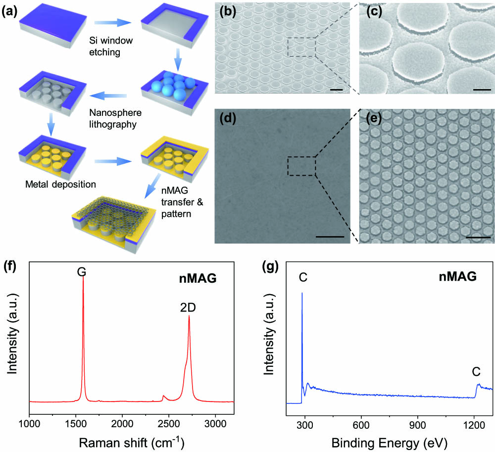
    Fig. 1. Plasmonic-enhanced nMAG–Au–Si nanostructure architecture. (a) Schematic of the nMAG–Au–Si nanostructure fabrication process using the nanosphere lithography method. (b), (c) Oblique view SEM images of the Si cylinder with the metallic nanostructure. The top–bottom metallic layer was deposited by 3 nm Ti and 30 nm Au. (d) Top view SEM image of the nMAG transferred on the metallic nanostructures. (e) Close-up SEM image of the area outlined by the dashed box in panel (d) shows the metallic coupled plasmon covered by nMAG film. The scale bars are 1 μm, 300 nm, 100 μm, and 2 μm in panels (b)–(e), respectively. (f) Raman spectrum of nMAG. (g) X-ray photoelectron spectroscopy (XPS) profile of the nMAG with no detectable oxygen peak (531.5 eV). C represents the carbon peak.
    Device structural characterization of the dual-band IR photodetector. (a) Schematic of the nMAG–Au–Si device showing the charge transport and the surface plasmon polariton coupled to the nMAG. The top schematic diagram shows the absorbance of the dual-band photodetector. (b) Wavelength-dependent properties of experimental (solid blue line) and simulated (red dashed line) reflection spectra. (c), (d) Current as a function of the bias voltage under laser illumination at 1342 nm and 1850 nm under different excitation power, respectively.
    Fig. 2. Device structural characterization of the dual-band IR photodetector. (a) Schematic of the nMAG–Au–Si device showing the charge transport and the surface plasmon polariton coupled to the nMAG. The top schematic diagram shows the absorbance of the dual-band photodetector. (b) Wavelength-dependent properties of experimental (solid blue line) and simulated (red dashed line) reflection spectra. (c), (d) Current as a function of the bias voltage under laser illumination at 1342 nm and 1850 nm under different excitation power, respectively.
    Mechanism for the enhancement electric field of the nMAG–Au–Si photodetector. (a)–(d) Simulated electric field distribution of the nanostructure-based device under illumination with the wavelengths of 1175, 1342, 1850, and 1990 nm, respectively.
    Fig. 3. Mechanism for the enhancement electric field of the nMAG–Au–Si photodetector. (a)–(d) Simulated electric field distribution of the nanostructure-based device under illumination with the wavelengths of 1175, 1342, 1850, and 1990 nm, respectively.
    Optoelectric characteristics of the plasmonic nanostructure-based photodetector with enhanced photoresponse. (a) The band diagram is associated with the hot-carrier generation by the PTI effect and SPR-induced process under infrared light optical excitation of the nMAG–Au–Si photodetector. (b), (c) Photocurrent as a function of different incident power densities with (red squares) and without (blue triangles) nanostructures under the bias of −1 V at the wavelengths of 1342 nm and 1850 nm, respectively. The data are fitted with a power law Iph∼Pβ, and the corresponding fitting results were represented as dashed lines of the same color as the data sets. (d) Relationship between responsivity (pink scatter) and external quantum efficiency (EQE) (lavender line and scatter) under increasing power density at 1342 nm (squares) and 1850 nm (triangles). (e) Noise power spectral density (NSD) SI of the nMAG–Au–Si vertical structure under various voltage bias conditions.
    Fig. 4. Optoelectric characteristics of the plasmonic nanostructure-based photodetector with enhanced photoresponse. (a) The band diagram is associated with the hot-carrier generation by the PTI effect and SPR-induced process under infrared light optical excitation of the nMAG–Au–Si photodetector. (b), (c) Photocurrent as a function of different incident power densities with (red squares) and without (blue triangles) nanostructures under the bias of 1  V at the wavelengths of 1342 nm and 1850 nm, respectively. The data are fitted with a power law IphPβ, and the corresponding fitting results were represented as dashed lines of the same color as the data sets. (d) Relationship between responsivity (pink scatter) and external quantum efficiency (EQE) (lavender line and scatter) under increasing power density at 1342 nm (squares) and 1850 nm (triangles). (e) Noise power spectral density (NSD)  SI of the nMAG–Au–Si vertical structure under various voltage bias conditions.
    Hot-carrier transport in nMAG. (a) 2D transient absorption mapping of nMAG on BaF2 as functions of probe delay time and the incident photon energy. (b) Normalized differential transmittance of the sample under pump light of 1550 nm under 1 mW/mm2. The signal was probed and collected at 1342 nm.
    Fig. 5. Hot-carrier transport in nMAG. (a) 2D transient absorption mapping of nMAG on BaF2 as functions of probe delay time and the incident photon energy. (b) Normalized differential transmittance of the sample under pump light of 1550 nm under 1  mW/mm2. The signal was probed and collected at 1342 nm.
    Specific detectivity (D*) and transient response time of the nanostructure photodetector. (a) D* and noise-equivalent-power (NEP) as a function of the varying power density under the illumination of 1342 nm. (b) Normalized photoresponse under the different frequencies from 1 Hz to 500 kHz illuminated with the CW 1342 nm laser capable of TTL on/off modulation, indicating the −3 dB bandwidth of 290 kHz. (c) Rising and falling times are obtained from the inset: time-dependent photocurrent of the device with a power density of 200 mW cm−2 with the frequency of 100 kHz under the illumination of 1342 nm. The response times are extracted within the photocurrent level of 10%–90%. (d) Photoresponse of the device with varying power conditions under 1342 nm laser modulated by the frequency of 100 kHz.
    Fig. 6. Specific detectivity (D*) and transient response time of the nanostructure photodetector. (a) D* and noise-equivalent-power (NEP) as a function of the varying power density under the illumination of 1342 nm. (b) Normalized photoresponse under the different frequencies from 1 Hz to 500 kHz illuminated with the CW 1342 nm laser capable of TTL on/off modulation, indicating the 3  dB bandwidth of 290 kHz. (c) Rising and falling times are obtained from the inset: time-dependent photocurrent of the device with a power density of 200  mWcm2 with the frequency of 100 kHz under the illumination of 1342 nm. The response times are extracted within the photocurrent level of 10%–90%. (d) Photoresponse of the device with varying power conditions under 1342 nm laser modulated by the frequency of 100 kHz.
    Xinyu Liu, Shaoxiong Wu, Xiaoxue Cao, Feng Tian, Srikrishna Chanakya Bodepudi, Muhammad Malik, Chao Gao, Li Peng, Huan Hu, Yang Xu, "Plasmon resonance-enhanced graphene nanofilm-based dual-band infrared silicon photodetector," Photonics Res. 11, 1657 (2023)
    Download Citation