Kun Liao, Tianyi Gan, Xiaoyong Hu, Qihuang Gong. On-Chip Nanophotonic Devices Based on Dielectric Metasurfaces[J]. Acta Optica Sinica, 2021, 41(8): 0823001
Search by keywords or author
- Acta Optica Sinica
- Vol. 41, Issue 8, 0823001 (2021)
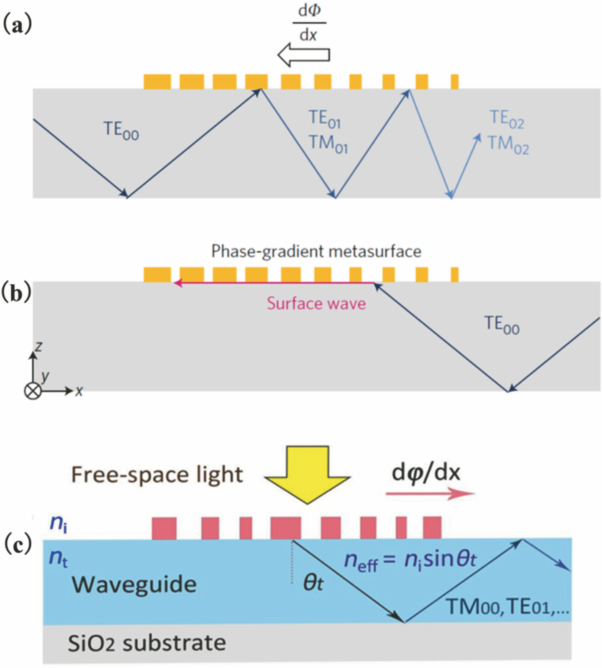
![Schematic diagrams of phase gradient control and phase matching. (a) Direction of light propagation is opposite to that of phase gradient[36]; (b) direction of light propagation is the same as that of phase gradient[36]; (c) coupling free light field into waveguide propagation mode by phase matching[40]](/richHtml/gxxb/2021/41/8/0823001/img_1.jpg)
Fig. 1. Schematic diagrams of phase gradient control and phase matching. (a) Direction of light propagation is opposite to that of phase gradient[36]; (b) direction of light propagation is the same as that of phase gradient[36]; (c) coupling free light field into waveguide propagation mode by phase matching[40]
![Schematic diagrams of devices using surface plasmon and mode converter. (a)(b) Structure diagrams of metal antenna array on one dimensional dielectric silicon nitride waveguide[47]; (c) schematic diagram of waveguide mode converter[52]](/richHtml/gxxb/2021/41/8/0823001/img_2.jpg)
Fig. 2. Schematic diagrams of devices using surface plasmon and mode converter. (a)(b) Structure diagrams of metal antenna array on one dimensional dielectric silicon nitride waveguide[47]; (c) schematic diagram of waveguide mode converter[52]
Fig. 3. Design of on-chip super surface lens using effective refractive index[46]. (a) Effective refractive indexes of gold blocks with different lengths varying with wavelength; (b) change of effective refractive index with the length of gold block at selected wavelength; (c) curve of effective refractive index at each point
Fig. 4. Structure schematic of metasurface design using transfer matrix. (a)(b) Schematic diagram of waveguide mode converter[52]; (c)(d) schematic diagram of antenna coupler for arbitrary polarization[39]
Fig. 5. Structural diagram of metasurface dispersionless lens[56]
Fig. 6. Schematic diagrams of metasurface beam splitter. (a) Schematic diagram of metasurface mode beam splitter[48] ; (b) for TE and TM modes, schematic diagrams of the effective refractive index of the metasurface[48] ; (c) electron micrograph of metasurface wavelength beam splitter[57] ; (d) transmission change of different channels with different wavelengths[57]
Fig. 7. Structure diagrams of metasurface on-chip coupler. (a) Structure diagram and electron microscope photo of photonic crystal structure coupler[41]; (b) schematic diagram of antenna structure coupler[39]
Fig. 8. Metasurface mode converter. (a) Schematic diagram of metasurface mode converter[55]; (b) transmission curves of various waveguide modes[55]; (c) electron micrograph of metasurface mode converter[52]; (d) mode conversion efficiency curves of various waveguide modes[52]
Fig. 9. Metasurface dispersionless lens and convolver[56]. (a) Electron micrograph of metasurface dispersionless lens; (b)(c) intensity distribution at focal plane of metasurface lens for 1000 nm and 1550 nm; (d)(e) theoretical calculation, numerical simulation and experimental results of metasurface convolver for 1000 nm and 1550 nm
Fig. 10. Asymmetric propagation waveguide[36]. (a) Structure diagram of asymmetric propagation waveguide; (b) transmission distribution of incident TE fundamental mode from the left; (c) transmission distribution of incident TE fundamental mode from the right

Set citation alerts for the article
Please enter your email address


