Fei Wang, Xiaochang Yu, Qingling Luo, Chengyang Zhou, Yiting Yu. Research Progress and Applications of Spectral Imaging System on Chip[J]. Laser & Optoelectronics Progress, 2021, 58(20): 2000002
Search by keywords or author
- Laser & Optoelectronics Progress
- Vol. 58, Issue 20, 2000002 (2021)
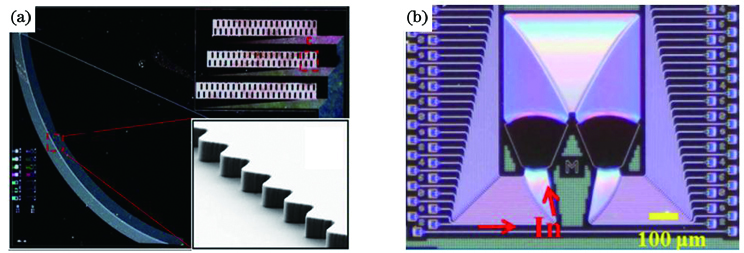
![Schematic diagrams of EDG and AWG. (a) Micrograph of EDG[5]; (b) schematic diagram of AWG[6]](/richHtml/lop/2021/58/20/2000002/img_1.jpg)
Fig. 1. Schematic diagrams of EDG and AWG. (a) Micrograph of EDG[5]; (b) schematic diagram of AWG[6]
![Fourier-transform spectral element diagram. (a) Micrograph of Fourier-transform chip-scale spectrometer [4]; (b) chip-scale speckle enhanced Fourier-transform spectrometer [13]](/richHtml/lop/2021/58/20/2000002/img_2.jpg)
Fig. 2. Fourier-transform spectral element diagram. (a) Micrograph of Fourier-transform chip-scale spectrometer [4]; (b) chip-scale speckle enhanced Fourier-transform spectrometer [13]
Fig. 3. FP filter. (a) Micrograph of 128×128 FP filter array produced by surface micro-machining[15]; (b) configuration of FP filter based on polymer-stabilized blue phase liquid crystals [16]
Fig. 4. Filter structures. (a) Multispectral filter array structures[19]; (b) true image of a linear variable filter working in 450--900 nm[20]
Fig. 5. Filtering structures. (a) Nanodisk-nanohole hybrid structure arrays; (b) ultrafine spectrum tunability[21]
Fig. 6. Products of detectors at home and abroad. (a) GST1212M detector of Wuhan Guide Infrared[22]; (b) ceramic package detector of IRay Technology[23]; (c) wafer level packaged detector of L-3 communications in America[24]; (d) UL03262 detector of ULIS in France[26]
Fig. 7. Methods of discrete-manufacturing-then-integrating. (a) Sony realized the integration of nano aluminum hole filter arrays and detector through manual operation under microscope[27]; (b) spectral chip manufactured by Zhejiang University based on wafer bonding technology[31]; (c) schematic diagram of FP filter structure and focal plane arrays integration through bonding [33]
Fig. 8. IMEC builds an extremely compact spectral imaging system based on FP interference filter chip[35]
Fig. 9. Integration of detector and filter. (a) Concept diagram of DARPA’s adaptive focal plane arrays [36]; (b) integration of detector and FP filter structure [37]
Fig. 10. Integrated filtering image sensor by IMEC. (a) Chip-scale multispectral imager through integrated per-pixel filtering by IMEC; (b) IMEC integrated filtering CMOS image sensor (left) and package (right) [39]
Fig. 11. Hyperspectral mobile application equipments. (a) Optical concept map of VTT iPhone 5s hyperspectral imager;(b) banknote recognition application based on iPhone 5s hyperspectral imager; (b1)-(b3) images of banknotes at 491 nm, 460 nm, and 521 nm, respectively, and the “tiny circle” pattern on the images is visible at 460 nm and 491 nm, but not at 521 nm[41]
Fig. 12. On-chip spectral imaging products. (a) Compact spectral imaging system of IMEC (top view at left and axonometric view at right); (b) white plastic articles group (left side is physical image, right side is spectrum obtained by the compact spectral imaging system)[35]
Fig. 13. Optical sorting by Ximea xiQ multispectral camera [50]
Fig. 14. Description and size of Specim IQ multi-spectral camera (left) and camera rendering (right) [52]

Set citation alerts for the article
Please enter your email address


