• Advanced Photonics
  • Vol. 3, Issue 2, 024001 (2021)
Dandan Wen1, Jasper J. Cadusch1, Jiajun Meng1, and Kenneth B. Crozier1、2、3、*
Author Affiliations
  • 1University of Melbourne, Department of Electrical and Electronic Engineering, Victoria, Australia
  • 2University of Melbourne, School of Physics, Victoria, Australia
  • 3University of Melbourne, Australian Research Council, Centre of Excellence for Transformative Meta-Optical Systems, Victoria, Australia
  • show less
    DOI: 10.1117/1.AP.3.2.024001 Cite this Article Set citation alerts
    Dandan Wen, Jasper J. Cadusch, Jiajun Meng, Kenneth B. Crozier. Light field on a chip: metasurface-based multicolor holograms[J]. Advanced Photonics, 2021, 3(2): 024001 Copy Citation Text show less
    Multicolor holograms that employ angular multiplexing. (a) Multicolor images generated by off-axis illumination of the metasurface hologram. The metasurface consists of nanoslits in a gold film. (b) Multicolor hologram that consists of nanoslits in an aluminum film. (c) Schematic of phase modulation by athermal photoreduction using a single fs pulse. A pulse passes through a parallel digitalization objective and generates a focal spot array with different intensities, which in turn leads to refractive-index modulation of the rGO composite. (d) Multicolor image generated by illuminating the metasurface with R, G, and B beams at different angles. The figures are reproduced with permission from (a) Ref. 70, (b) Ref. 71, (c), (d) Ref. 72.
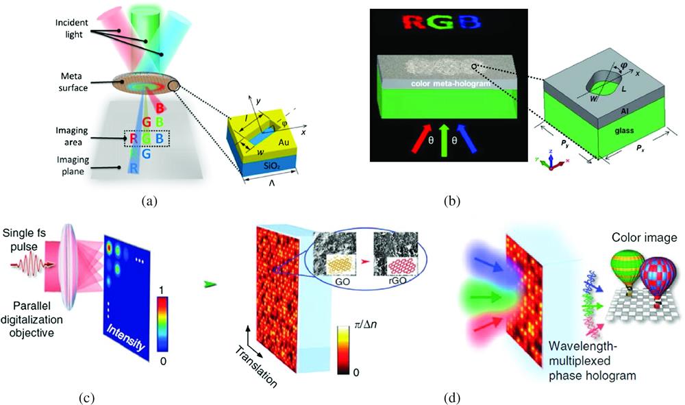
    Fig. 1. Multicolor holograms that employ angular multiplexing. (a) Multicolor images generated by off-axis illumination of the metasurface hologram. The metasurface consists of nanoslits in a gold film. (b) Multicolor hologram that consists of nanoslits in an aluminum film. (c) Schematic of phase modulation by athermal photoreduction using a single fs pulse. A pulse passes through a parallel digitalization objective and generates a focal spot array with different intensities, which in turn leads to refractive-index modulation of the rGO composite. (d) Multicolor image generated by illuminating the metasurface with R, G, and B beams at different angles. The figures are reproduced with permission from (a) Ref. 70, (b) Ref. 71, (c), (d) Ref. 72.
    Multicolor holograms by the polarization multiplexing method. (a) Design process for the vectorial color holographic metasurface. (b) Schematic of 6-bit metasurface. Holographic images that result from the state (color and polarization) of the incident light as denoted by codes 010000, 001000, 000100, 000110, 000101, 000011, 111000, and 001110 are shown in the right panel of the image. Figures reproduced with permission from (a) Ref. 64 and (b) Ref. 75.
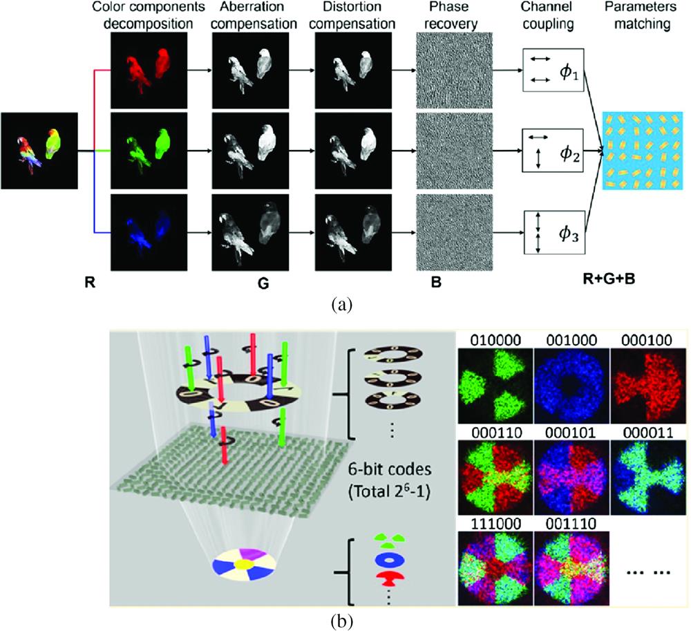
    Fig. 2. Multicolor holograms by the polarization multiplexing method. (a) Design process for the vectorial color holographic metasurface. (b) Schematic of 6-bit metasurface. Holographic images that result from the state (color and polarization) of the incident light as denoted by codes 010000, 001000, 000100, 000110, 000101, 000011, 111000, and 001110 are shown in the right panel of the image. Figures reproduced with permission from (a) Ref. 64 and (b) Ref. 75.
    Narrow band CP converters-based multicolor holograms. (a) Solid curves: simulated diffraction efficiency of three nanoblock types, denoted by SR, SG, and SB. The circle, square, and rectangle represent the simulated efficiency when the SR, SG, and SB are merged into the same pixel as shown in (b). (c) Schematic of multicolor image reconstruction. (d) Multicolor hologram in reflection mode. The metasurface consists of three types of silicon nanoblocks that work as narrow band CP converters. (e) Schematic of the polarization-controlled multicolor hologram. The figures are reproduced with permission from (a)–(c) Ref. 78, (d) Ref. 79, and (e) Ref. 63.
    Fig. 3. Narrow band CP converters-based multicolor holograms. (a) Solid curves: simulated diffraction efficiency of three nanoblock types, denoted by SR, SG, and SB. The circle, square, and rectangle represent the simulated efficiency when the SR, SG, and SB are merged into the same pixel as shown in (b). (c) Schematic of multicolor image reconstruction. (d) Multicolor hologram in reflection mode. The metasurface consists of three types of silicon nanoblocks that work as narrow band CP converters. (e) Schematic of the polarization-controlled multicolor hologram. The figures are reproduced with permission from (a)–(c) Ref. 78, (d) Ref. 79, and (e) Ref. 63.
    Color printing and holography by the narrow band CP converters. (a) Schematic of a shallow plasmonic grating. (b) Printed image observed with the white light microscope. This chip would be used with a “decryption device” that ensures that the incident light and the detected light are both CP with the same helicity. (c) Holographic image generated when the chip is illuminated by R, G, and B laser beams. (d) Schematics of a nanoblock (right) and a nanoblock dimer (left), which make up the metasurface. (e) Optical microscope image of the hologram when viewed under white light illumination. (f) Two-color (R & G) holographic image. (g) Unit cell of the metasurface hologram, containing two crystalline silicon nanoblocks. (h) Color printed image (left) and reconstructed holographic image (right). The figures are reproduced with permission from: (a)–(c) Ref. 80; (d)–(f) Ref. 81; (g), (h) Ref. 82.
    Fig. 4. Color printing and holography by the narrow band CP converters. (a) Schematic of a shallow plasmonic grating. (b) Printed image observed with the white light microscope. This chip would be used with a “decryption device” that ensures that the incident light and the detected light are both CP with the same helicity. (c) Holographic image generated when the chip is illuminated by R, G, and B laser beams. (d) Schematics of a nanoblock (right) and a nanoblock dimer (left), which make up the metasurface. (e) Optical microscope image of the hologram when viewed under white light illumination. (f) Two-color (R & G) holographic image. (g) Unit cell of the metasurface hologram, containing two crystalline silicon nanoblocks. (h) Color printed image (left) and reconstructed holographic image (right). The figures are reproduced with permission from: (a)–(c) Ref. 80; (d)–(f) Ref. 81; (g), (h) Ref. 82.
    Dispersion phase-based multicolor holograms. (a) Simulated reflectance spectra, with the nanorod length varied. (b) Simulated reflectance and phase at λ=405, 532, and 658 nm. Blue circles, green triangles, and red squares indicate the nanorod lengths used for the blue, green, and red channels, respectively. (c) Experimentally obtained color holographic image. (d) Unit cell of the multicolor hologram. (e) Calculated phases at wavelengths of 460, 540, and 700 nm. The color used for the data points represents the nanopillar width, as indicated by the colorbar. The star symbol (labeled “A”) represents an example of a target phase point, while the red dot (labeled “B”) represents the nanopillar that is closest to this target. (f) Simulated color holographic image produced by the metasurface. The figures are reproduced with permission from: (a)–(c) Ref. 85, (d)–(f) Ref. 86.
    Fig. 5. Dispersion phase-based multicolor holograms. (a) Simulated reflectance spectra, with the nanorod length varied. (b) Simulated reflectance and phase at λ=405, 532, and 658 nm. Blue circles, green triangles, and red squares indicate the nanorod lengths used for the blue, green, and red channels, respectively. (c) Experimentally obtained color holographic image. (d) Unit cell of the multicolor hologram. (e) Calculated phases at wavelengths of 460, 540, and 700 nm. The color used for the data points represents the nanopillar width, as indicated by the colorbar. The star symbol (labeled “A”) represents an example of a target phase point, while the red dot (labeled “B”) represents the nanopillar that is closest to this target. (f) Simulated color holographic image produced by the metasurface. The figures are reproduced with permission from: (a)–(c) Ref. 85, (d)–(f) Ref. 86.
    Detour phase-based metasurface consisting of color holograms encoded into color printed images. (a) Schematic of a TiO2 nanocone array that comprises the metasurface. Each cone has height h, period p, top radius r, and taper angle β. (b) Illustration of the detour phase concept. Each supercell has width Δx and length Δy. δx is the distance of the cone array from the supercell center. The detour phase of each pixel is controlled by δx. (c), (d) Optical image of the metasurface captured by the polarization microscope. The outer diameter of the pattern in (c) is 1.5 mm. The scalebar in (d) represents 50 μm. (e) Reconstructed holographic image with sample A, whose optical image is shown in (c). (f) Reconstructed holographic image with sample B, whose optical image is similar to (c). Color bars in (e) and (f) both represent 5 cm. The figures are reproduced with permission from (a)–(f) Ref. 66.
    Fig. 6. Detour phase-based metasurface consisting of color holograms encoded into color printed images. (a) Schematic of a TiO2 nanocone array that comprises the metasurface. Each cone has height h, period p, top radius r, and taper angle β. (b) Illustration of the detour phase concept. Each supercell has width Δx and length Δy. δx is the distance of the cone array from the supercell center. The detour phase of each pixel is controlled by δx. (c), (d) Optical image of the metasurface captured by the polarization microscope. The outer diameter of the pattern in (c) is 1.5 mm. The scalebar in (d) represents 50  μm. (e) Reconstructed holographic image with sample A, whose optical image is shown in (c). (f) Reconstructed holographic image with sample B, whose optical image is similar to (c). Color bars in (e) and (f) both represent 5 cm. The figures are reproduced with permission from (a)–(f) Ref. 66.
    Monolithically integrated metasurfaces that consist of a color filter layer and a phase-only hologram layer. (a) Schematic of the pixel that functions as both a color filter (via nanopillars) and as a phase plate (via thin film under the pillars). (b) Transmission optical micrograph of a color printed image. It contains six colors: red, green, blue, orange, yellow, and purple. (c)–(e) Holographic images produced by illumination with R, G, and B laser beams. (f) Schematic of a metasurface unit cell. The Ag-HSQ-Ag cavity serves as a transmission-type color filter. PMMA nanoholes control the phase of transmitted light. The PMMA layer is separated from the color filter by an HSQ layer. (g) Simulated and experimentally measured transmission spectra of R, G, and B color filters. These are optimized for operation at 450, 532, and 633 nm. The solid/dashed darker blue curves represent experimental/theoretical transmission spectra when the Ag layers (both top and bottom Ag layers in MIM filter) are 26 nm and the total filter height is 93 nm. The thickness of the Ag layer and the height of the structure are listed for the other cases: 26 nm/126 nm (darker green curves), 26 nm/161 nm (darker red curves), 31 nm/95 nm (lighter blue curves), 31 nm/128 nm (lighter green curves), and 31 nm/164 nm (lighter red curves). (h) Color holographic image produced by illumination of metasurface with R, G and B laser beams. The image is of James Clerk Maxwell, with the different colors achieved via mixtures of R, G, B components. The figures are reproduced with permission from: (a)–(e) Ref. 65, (f)–(h) Ref. 93.
    Fig. 7. Monolithically integrated metasurfaces that consist of a color filter layer and a phase-only hologram layer. (a) Schematic of the pixel that functions as both a color filter (via nanopillars) and as a phase plate (via thin film under the pillars). (b) Transmission optical micrograph of a color printed image. It contains six colors: red, green, blue, orange, yellow, and purple. (c)–(e) Holographic images produced by illumination with R, G, and B laser beams. (f) Schematic of a metasurface unit cell. The Ag-HSQ-Ag cavity serves as a transmission-type color filter. PMMA nanoholes control the phase of transmitted light. The PMMA layer is separated from the color filter by an HSQ layer. (g) Simulated and experimentally measured transmission spectra of R, G, and B color filters. These are optimized for operation at 450, 532, and 633 nm. The solid/dashed darker blue curves represent experimental/theoretical transmission spectra when the Ag layers (both top and bottom Ag layers in MIM filter) are 26 nm and the total filter height is 93 nm. The thickness of the Ag layer and the height of the structure are listed for the other cases: 26  nm/126  nm (darker green curves), 26  nm/161  nm (darker red curves), 31  nm/95  nm (lighter blue curves), 31 nm/128 nm (lighter green curves), and 31  nm/164  nm (lighter red curves). (h) Color holographic image produced by illumination of metasurface with R, G and B laser beams. The image is of James Clerk Maxwell, with the different colors achieved via mixtures of R, G, B components. The figures are reproduced with permission from: (a)–(e) Ref. 65, (f)–(h) Ref. 93.
    Multicolor holograms realized with binary/complex amplitude modulation. (a) Design process for a multicolor hologram consisting of circularly and elliptically shaped silver particles. (b) Two-color holographic image produced by illumination of a metasurface with red and blue laser beams. (c) Schematic of a metasurface waveguide system. R, G, and B laser beams are coupled into a waveguide by a grating coupler. (d) Holographic image produced by a metasurface waveguide system. R, G, and B light in waveguides is coupled out into free space by the grating-based metasurface to form the holographic image. (e) Unit cell of the device termed a “multifreedom metasurface” by Deng et al.95" target="_self" style="display: inline;">95 Amplitude, phase, and polarization of the reflected light can be controlled by the parameters p1, p2, ψ1, and ψ2. (f) Simulated (left) and experimentally obtained (right) holographic images. The figures are reproduced with permission from (a), (b) Ref. 96, (c), (d) Ref. 97, (e), (f) Ref. 95.
    Fig. 8. Multicolor holograms realized with binary/complex amplitude modulation. (a) Design process for a multicolor hologram consisting of circularly and elliptically shaped silver particles. (b) Two-color holographic image produced by illumination of a metasurface with red and blue laser beams. (c) Schematic of a metasurface waveguide system. R, G, and B laser beams are coupled into a waveguide by a grating coupler. (d) Holographic image produced by a metasurface waveguide system. R, G, and B light in waveguides is coupled out into free space by the grating-based metasurface to form the holographic image. (e) Unit cell of the device termed a “multifreedom metasurface” by Deng et al.95 Amplitude, phase, and polarization of the reflected light can be controlled by the parameters p1, p2, ψ1, and ψ2. (f) Simulated (left) and experimentally obtained (right) holographic images. The figures are reproduced with permission from (a), (b) Ref. 96, (c), (d) Ref. 97, (e), (f) Ref. 95.
    Dandan Wen, Jasper J. Cadusch, Jiajun Meng, Kenneth B. Crozier. Light field on a chip: metasurface-based multicolor holograms[J]. Advanced Photonics, 2021, 3(2): 024001
    Download Citation