Silvia Romano, Gianluigi Zito, Stefania Torino, Giuseppe Calafiore, Erika Penzo, Giuseppe Coppola, Stefano Cabrini, Ivo Rendina, Vito Mocella, "Label-free sensing of ultralow-weight molecules with all-dielectric metasurfaces supporting bound states in the continuum," Photonics Res. 6, 726 (2018)
Copy Citation Text
The realization of an efficient optical sensor based on a photonic crystal metasurface supporting bound states in the continuum is reported. Liquids with different refractive indices, ranging from 1.4000 to 1.4480, are infiltrated in a microfluidic chamber bonded to the sensing dielectric metasurface. A bulk liquid sensitivity of 178 nm/RIU is achieved, while a -factor of about 2000 gives a sensor figure of merit up to 445 in air at both visible and infrared excitations. Furthermore, the detection of ultralow-molecular-weight (186 Da) molecules is demonstrated with a record resonance shift of 6 nm per less than a 1 nm thick single molecular layer. The system exploits a normal-to-the-surface optical launching scheme, with excellent interrogation stability and demonstrates alignment-free performances, overcoming the limits of standard photonic crystals and plasmonic resonant configurations.
Optical sensors can reveal layer thickness changes, bulk fluid properties, molecular bindings, or cellular interactions by measuring changes of the refractive index (RI), light absorption, or scattering at the sensing surface. Surface plasmon resonance (SPR) and localized surface plasmon resonance (LSPR) sensors are considered a gold standard in label-free and real-time surface sensing [1–4]. The large spectral shift of the resonance peak in response to a relatively small change of the refractive index of the surrounding medium corresponds to high values of the bulk sensitivity [5–7]. However, the figure of merit (where FWHM is the full width at half maximum) of plasmonic sensors reaches around 8 [8,9] for LSPR-based sensors and around 23 [9] for SPR devices, being strongly limited by the large plasmonic resonance linewidth due to the high optical absorption losses in the metal. Low values of FOM negatively affect the performance of a sensing device and the limit of detection. In complex plasmonic metamaterial-based sensors, large sensitivity can be reached. FOM values of 330 have been reported [10]. A high FOM value is typically associated with large -factors, for which engineering of complex designs is mandatory. In this regard, several efforts have been put forward relying on Fano resonance engineering, yet mainly in the case of plasmonic structures [11]. These last are affected by optical losses in the visible range and are more efficient in the terahertz range [12], where resistive losses are minimal. However, in this case, detector efficiency is poor, and a large footprint may be a technological limitation.
A promising class of optical sensors characterized by a high -factor and large values of FOM is based on photonic crystal (PhC) nanocavities [13]. They typically consist of punctual defects in a PhC lattice [14] and provide strong interaction between the confined optical field and the analyte, finding direct application in the realization of gas, liquid, temperature, stress, humidity, refractive index, biochemical sensors, etc. [15–17]. However, a PhC cavity requires a high-precision nanofabrication process for controlling position and size of the air holes and precise near-field coupling [18,19], for instance, as with optical fiber coupling [20].
Herein, we explore a different sensing scheme approach overcoming the aforementioned limits. The device is based on plasmon-like surface waves, delocalized on a wide area to provide a large interaction volume with matter but excited in an all-dielectric photonic crystal metasurface (PhCM). It exploits a normal-to-the-surface optical launching scheme to easily excite high -factor resonances associated with bound states in the continuum (BICs) [21–27]. We characterize its sensing performances and analyze the capability of the metasurface resonance, showing a large near-field amplification, to sense the perturbation of the dielectric environment. BICs are resonances with a theoretical ideal infinite lifetime. These waves remain localized, even though they coexist with a continuous spectrum of radiating waves because of symmetry mismatch or topological constraints [28]. BICs behave as extended surface waves. The optical field remains confined along the direction perpendicular to the periodicity plane at the interfaces between the photonic crystal surface and the environment. This involves narrow resonances (high -factor) and large field intensity enhancement. A recent theoretical study has revealed the possibility of even 6 orders of magnitude amplification of the intensity in the near-field zone [29], demonstrating further possible application in fluorescent-based sensing configurations. Structures supporting BICs are actually distributed cavities with a natural high -factor, which also find direct application in lasing and filtering [30,31]. Fabrication imperfections and the finite extent of the structure break the ideality of the system, allowing far-field excitation in the near BIC regime.
Sign up for Photonics Research TOC. Get the latest issue of Photonics Research delivered right to you!Sign up now
In more detail, we demonstrate a BIC-based sensor having a -factor () large enough for demanding sensing applications [32,33], with the challenging capability of detecting ultralow-molecular-weight molecules (186 Da) [34]. Low-molecular-weight molecule recognition is extremely difficult [35], but the intense optical field at the surface and the intrinsic loss-free operation make these PhCM structures extremely sensitive to external environment perturbations. We measured a record resonance shift of 6 nm produced by the surface adsorption of a submonolayer of molecules with of thickness. In addition, this new class of devices exhibits good far-field light coupling in the near-BIC regime. In contrast with other standard planar PhC structures, it requires extremely simple interrogation equipment and minimal alignment procedures and, being a distributed cavity, is not affected by fabrication imperfection. The large sensing area () is a further characteristic extending the range of possible applications of the device. Finally, the results demonstrate a novel strategy for challenging biomolecular optical sensing.
2. RESULTS AND DISCUSSION
A. PhCM Design and Fabrication
In the first place, numerical simulations of the excited modes in the structure were carried out by using a full 3D rigorous coupled wave approach [36,37] based on Fourier modal expansion and finite-difference time-domain (FDTD) simulations using the commercial software FULLWAVE [38]. Finite-element-method-based simulations, carried out with COMSOL Multiphysics 5.2a, were also used to verify the consistency of all simulations and results (see Fig. 1).
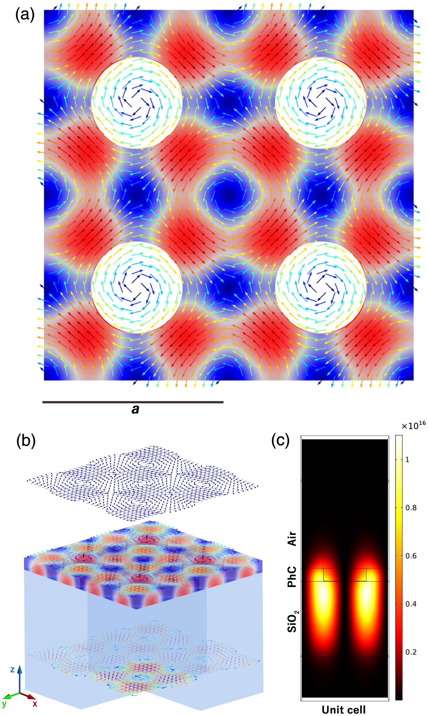
Figure 1.(a) Calculated electric field in resonance condition at the BIC mode at the -point of the Brillouin zone; top view of four unit cells with lattice constant . (b) BIC amplitude over the PhCM with superimposed arrow maps of the electric field; as clearly visible, the electric field forms a lattice of vortices and antivortices that cannot couple to radiating waves, revealing the bound-in-the-continuum character of the calculated mode. (c) Intensity profile of the electric field (side view of one unit cell) showing that the BIC wave is mostly confined at the interface , but the electromagnetic field enhancement at interface is expected to be large enough to provide strong light–matter interaction. Intensity enhancement of the simulation diverges in agreement with an ideal diverging -factor of an infinite structure.
We considered a PhCM of silicon nitride, at 780 nm, with a square lattice of period and thickness on a supporting quartz substrate with air as the top dielectric environment. The computational domain was limited to a unit cell of the PhCM. We applied Bloch periodic boundary conditions to surfaces along the and directions. On the top and bottom surfaces, normal to the direction [see Fig. 1(b)] and far enough from the metasurface, we imposed perfectly matched layer absorbing boundary conditions [38–40]. The adapted mesh along had a size-step of 3 nm inside the PhCM and increased outside, up to a value of 20 nm.
As shown in Fig. 1(a), the representative calculated nondegenerate BIC mode has the symmetries of the lattice and thus is a symmetry-protected BIC. This occurs when at normal incidence, where is the free-space wavelength of the mode. Also degenerate mode bands can provide high -factors as a result of the resonance-trapping BIC mechanism [30]. In general, at normal incidence (highly symmetric point) both symmetry-protection-based decoupling from continuum and resonance-trapping mechanisms might coexist in the same structure [30]. In Figs. 1(a) and 1(b), we show the electric field arrow map superimposed with amplitude distribution (blue to red color map). As visible in the figure, the field appears as a lattice of vortices and antivortices also in the region of air and in the bottom substrate [Fig. 1(b)], which, together with the evanescent character of the field mode, confirms that there is no possible energy flow to propagating waves for an ideal structure. Besides the specific nature of the decoupling mechanism, what is important to our purposes is that the BIC wave is an infinitely extended Bloch wave in the plane but is tightly confined in the direction, perpendicular to the periodicity plane, inside the PhCM. The field is evanescent in both directions, and the amplification of the near-field reaches values as large as , with input field amplitude. This feature suggests the possibility of strong light–matter interaction for sensing applications. When the radiation is ideally trapped within the structure, photons can accumulate, and the field value increases accordingly. Of course, in any real physical situation, there are loss channels like nonzero finite material absorption, scattering loss due to imperfections and roughness of the real geometry, fluctuation density of the materials, and finite lateral extension of the structure. Experimentally, the resonance will be close to an ideal BIC mode (which gives a Fano-like resonance profile). Likely, amplification values comparable with plasmonic resonances can be reached or even surpassed.
The sample consisted of cylindrical air holes in a square lattice, patterned in silicon nitride film. The layer was deposited on a substrate (120 µm of thickness) by plasma-enhanced chemical vapor deposition ( and ). It is worth stressing that silicon nitride deposited under realistic conditions may contain hydrogen impurities. As such, the actual layer composition typically deviates from the standard formula, which, however, does not change significantly the refractive index of the material. The design was patterned on the silicon nitride by means of electron beam lithography, and it was then transferred by means of the coupled plasma etching process using and . The lattice parameters were optimized in order to excite the BIC resonance at 780 nm. Specifically, the lattice constant was , the hole radius was , and the hole depth is [see Fig. 2(a)]. A microfluidic chamber was integrated into the device in order to infiltrate different refractive index liquids while monitoring in real-time the resulting position of the resonance wavelength. A sketch of the final device is shown in Fig. 2(b). The microfluidic chamber was fabricated using a PDMS (polydimethylsiloxane) soft-lithography technique [41] and consisted of a circular chamber with a diameter of 2 mm. The negative mold was obtained by spinning the KMPR 1050 at 1000 r/min in order to obtain a thickness of 100 µm. Then, the PDMS base and the curing agent were mixed in a ratio of ∶ and poured on the mold. The sample was placed on a hot plate at 100°C for 30 min. The cured polymers were peeled off the mold, and two holes were punched inside the chamber in order to allow the inflow and outflow of the solution. Finally, the chamber was bonded to the PhCM surface by means of a plasma process. The liquid flow was controlled by means of a syringe infusion pump (KD Scientific), allowing us to monitor the total infusion volume.
Figure 2.(a) Scanning electron microscopy image of the PhCM sample. The design consists of air cylindrical holes arranged in a square lattice (, , ). (b) Sketch of the device: a PDMS microfluidic chamber was bonded to the PhCM. The inlet and outlet allow the controlled injection of the fluid.
The same sensing mechanism was adopted also to detect small numbers of biphenyl-4-thiol (BPT) molecules, having ultralow molecular weight (186 Da), adsorbed over the sensor surface. Once infiltrating the chamber with a 1 µM (1 M = 1 mol/L) ethanol solution of BPT, this was left a few minutes to adsorb to the surface. Once the maximum shift in the transmission spectrum was detected, the chamber was repeatedly rinsed with pure ethanol to ensure the adsorption at most of a single monolayer, and then the sample was dried with air. Final measurements with adsorbed BPT reported here were carried out in air at the end of the process. No degradation of the sample surface was observed after molecular adsorption and rinsing as verified by atomic force microscopy (AFM) inspection.
B. Optical Characterization
The fabricated PhCMs, without the micro-chamber, were optically characterized by means of a dedicated optical setup [Fig. 3(a)]. Transmission spectra were acquired from the sample illuminated by a normally incident supercontinuum laser (NKT Photonics) by means of an Ocean Optics USB4000 spectrometer with a resolution of 0.25 nm. A computer-controlled rotational stage allowed us to perform angle-resolved measurements with a resolution of 0.01°. The transmitted light was filtered in crossed-polarization with respect to the incident beam so as to suppress the supercontinuum background. At the resonance, forward scattered light is partly polarized with a polarization component perpendicular to the excitation polarization, while the remaining part of the spectrum preserves its incident polarization properties. Thus, the near-BIC resonance appears as a peak in the forward scattering spectrum through the PhCM (otherwise, it would appear as a dip in the transmittance spectrum). Narrow peak resonances were detected in the transmission spectrum at normal incidence. We estimated an FWHM at the limits of the spectrometer resolution [see Fig. 4(a)]. The quality factor, ( linewidth, resonance frequency), was estimated by fitting the measured peak spectral profile with a Lorentzian line shape given by [42]
Figure 3.(a) Sketch of the experimental setup. SC source, supercontinuum source; , Glan–Thompson polarizer; R, automatic rotational stage; PhC, photonic crystal sample; , Glan–Thompson polarizer; S, spectrometer. (b) Experimental reconstructed band collected for p-polarized incident beam.
Figure 4.(a) BIC resonance excited in the PhC metasurfaces without the micro-chamber by a normally incident incoming beam. By fitting the measured spectrum (blue dots) with a Lorentzian line shape (purple curve), a linewidth and a quality factor as large as and , respectively, were determined. (b) Two measured transmitted spectra collected from the sensor device corresponding to different RI. (c) Reconstructed sensitivity curve; the linear fit (red curve) to the experimental data (blue dots) revealed a bulk sensitivity (R-square 0.99). Error bars refer to spectrometer resolution, whereas the statistical error on spectral peak position is within the size of the symbols. (d) Sensitivity curves corresponding to (red dots), (black squares), and (blue triangles). The sensitivities determined by linearly fitting the data were found close to each other.
A linewidth and a quality factor as large as (where is the speed of light) and , respectively, were determined. Angular-resolved measurements allowed us to reconstruct the dispersion band of the PhCM. In Fig. 3(b), the experimental p-mode dispersion band diagram is shown. At the point (), it is possible to appreciate a doubly degenerate band that splits into two curves when the incidence angle is slightly greater than . We actually measured the transmission spectra up to . Moving away from the highly symmetric point, the mode turns into a leaky mode, but the -factor was still rather large; however, the FOM was affected because of the linewidth broadening of a factor .
Bulk measurements. Following the measurements in air, the PDMS chamber was bonded to the silicon nitride PhCM, and Cargille certified refractive index liquids (SPI supplies) were infiltrated above the surface. The corresponding resonant mode for each liquid was detected recording the spectral profile and peak position by means of the spectrometer, as a function also of the incidence angle for small values around the -point. The results are reported in Fig. 4. When the RI changed from 1.4000 to 1.4480, the whole spectrum shifted toward the red [Fig. 4(b)]. As visible in the figure, two resonances were detected for each spectrum. This is likely due to the mechanical stress induced by the presence of the PDMS chamber that slightly changed the system with respect to the normal incidence condition in air, so the band splits into two modes [as highlighted in Fig. 3(b)]. As expected, infiltrating the liquid above the PhCM produced a broadening of the resonance linewidth, worsening the -factor. In addition, the resonance became asymmetric, and the Lorentzian model was substituted with a Fano asymmetric line shape for fitting. The asymmetry is ascribed to the coupling of the discrete in-plane state (confined resonant mode) with the continuum of vertical radiation modes, which may depend on the refractive index of the surrounding material. By monitoring the first peak of the spectrum as a function of the solution RI, the sensitivity curve was reconstructed [Fig. 4(c)]. The relation between the RI variation of the fluid and the resonance shifts was linear. The fit parameters to the experimental data revealed a bulk sensitivity [Fig. 4(c)]. A linewidth was estimated by fitting the resonance with an asymmetric line shape [42], with complex number.
An important comparative parameter of sensing devices is the FOM, which takes into account the sharpness of the resonance and thus examines the ability to sensitively measure tiny wavelength changes. This parameter reaches around 8 [8,9] for LSPR-based sensors and around 23 [9] for SPR devices. In complex plasmonic metamaterial-based sensors, FOM values of 330 have been reported [10]. Our BIC-based sensor led to an FOM of 445 in air and of 297 in liquid, which are comparable with state-of-the-art values obtained with hyperbolic metamaterial nanosensors [35]. Reduction of the FOM in liquid is due to the broadening of the resonance ascribed to larger scattering losses, minor dielectric contrast, and lower degree of collimation of the input laser beam. The large FOM of our sensor allows us to appreciate variations of the order of the instrumental spectral resolution. By using an accurate optical spectrum analyzer with a resolution of 0.05 nm, the limit of detection is estimated conservatively in a minimal variation of RI of . As for SPR, more sophisticated fitting procedures [43] may lead to a spectral precision as large as , improving by 2 orders of magnitude our estimated limit of detection. In order to provide a more direct comparison, following the general discussion of PhC nanocavity sensitivity, let us consider the detection limit () of the PhCM-based RI sensor. It can be calculated by the measurement sensitivity () and the minimal resolvable wavelength shift () and is given by relation . For a resonance, the relationship between and quality factor is [13]. Thus, . This again corresponds to a value RIU for our PhCM-BIC sensor, which is comparable with highly performing PhC cavity sensors [13,44,45]. However, two advantages of the BIC-sensing scheme developed here may be useful for several applications such as cell membrane processes sensing.
(i) In practical applications of PhC nanocavity sensors, one challenge is the poor far-field light coupling and large area sensing [46]. Coupling requirements are nowadays typically solved in moderate to high-volume telecom applications, although far-field direct coupling would facilitate integration and less complex designs. In contrast with PhC nanocavity sensors, our BIC-based sensor largely facilitates alignment procedures thanks to a simple and extremely efficient far-field coupling in the near-BIC regime (80%) and its distributed cavity-sensing principle; indeed, cavity confinement is in the transverse direction and is not affected by fabrication imperfection.
(ii) Typically, efficient PhC nanocavities or vertical cavity sensors [47] require large dielectric contrasts; thus, they are commonly made of silicon or other nontransparent materials to visible wavelengths. In contrast, our BIC-based sensor is made of silicon nitride, which is a transparent, low-loss material to visible wavelengths; thus, the interrogation scheme is extremely simplified and opens the avenue to a large variety of sensing schemes for correlative experiments requiring simultaneous multiplexed monitoring or transmission light microscopy. Thus, our experimental approach provides major differences in the choice of material (transparent and bio-compatible) and the large sensing area, which are necessary in many cases in the biological field.
A possible issue of light coupling to the PhCM in the near-BIC regime is related to the precise angle definition [30]. However, in order to verify the independence of the sensitivity from the incidence angle of interrogation, angle-resolved measurements were performed. The sensitivity curves were determined by acquiring the transmission spectra corresponding to different incident angles of the incoming beam, which resulted in a rigid translation of the resonant peaks [Fig. 4(d)]. The sensitivity values , , and , respectively, corresponding to , , and , were found close to each other, demonstrating that no particular care had to be taken to align the beam along the normal incidence. This feature is consistent with the properties of a resonance-trapped BIC, i.e., a degenerate band mode at , for which the -factor remains large even far from the high symmetric -point [30]. It is worth mentioning that, even though the PhCM band diagram is symmetric with respect to the -point, the PDMS chamber bonded to the PhCM can break the ideal symmetry, introducing a slight refraction effect, which explains the small discrepancy between the sensitivity values at .
It is worth underlining that our sensor is highly versatile and can work in different spectral ranges. In order to demonstrate this, the same measurements were performed in the visible range on a suitably designed photonic crystal metasurface. In particular, mixtures of water and isopropyl alcohol at several ratios were infiltrated in the micro-chamber. The peak resonance shift was monitored as a function of refractive index change for increasing concentration of isopropyl alcohol (Fig. 5). The resulting sensitivity was found close to the infrared interrogation case discussed above; indeed, we estimated a sensitivity of 185 nm/RIU.
Figure 5.Reconstructed sensitivity curve in the visible range; the measurements demonstrated the scalability of the device, which reveals a bulk sensitivity (R-square 0.96).
Surface measurements. A remarkable feature of the BIC mode relies on its surface wave nature, i.e., the electromagnetic confinement in the near-field of the PhCM, as shown in Fig. 1. The field decays over a length scale of the order of 100 nm and is therefore mainly sensitive to the material properties of the region close to the surface or attached to it at the boundary, as for LSPR sensors. A significant advantage of the BIC mode with respect to the LSPR in metal sensors is the perfect transparency of the dielectric material of the PhCM (silicon nitride) and thus the absence of heating due to the metal absorption. To demonstrate the PhCM surface sensitivity, we soaked the dielectric structure in a 1 µM solution of BPT in ethanol, infiltrated in the microfluidic chamber. BPT is a small molecule with an ultralow molecular weight, 186 Da. It self-assembles on gold structures, leaving a monolayer of molecules with a surface density of two molecules per , with a thickness . In the case of our dielectric structure, however, less than a monolayer is estimated because no covalent bonding of the BPT to silicon nitride forms. After soaking in the BPT-ethanol solution, the chamber is rinsed for several times with pure ethanol and then left to dry in air. The optical microscopy inspection revealed no grains formation or impurities.
Because the BIC is highly confined at the boundary, it is extremely sensitive to the surface refractive index modification. Figure 6 shows the cross-polarized transmission spectrum of the PhCM prior and post-functionalization with the self-assembling monolayer of BPT. When the BPT monolayer is assembled, a redshift at the resonance wavelengths 1 and 2 occurred. We measured a state-of-the-art sensitivity of 6 nm of shift after the BPT monolayer formation, which is a remarkable result considering its low polarizability and limited thickness. For comparison, it is worth mentioning that record shifts achievable in LSPR nanobiosensors for monolayer formation are of the order of but solely with heavy protein binding. Indeed, the plasmonic resonance-based approach has poor sensitivity for detecting small analytes (), an issue that hampers modern requirements of biotechnology toward new nanoscale designs [10].
Figure 6.Cross-polarized transmission spectrum of the PhCM-based sensor prior (black curve) and post-functionalization with the self-assembling monolayer of BPT (red curve). When the BPT monolayer is assembled, a redshift at resonance wavelengths 1 and 2 occurred. A sensitivity of 6 nm of shift after the BPT monolayer formation was measured.
We carried out simulations as a function of the thickness of a top uniform dielectric layer with a refractive index of 1.45. The refractive index selected is an average value of the refractive indices of hydrocarbons and thiols (hexadecane 1.4345, decanethiol 1.4509, dodecanethiol 1.4589, and octadecanethiol 1.4645). The theoretical resonance shift was consistent with the experimental results, although our simulations were limited to a layer thickness larger than 5 nm for technical issues related to the number of degrees of freedom required for a fine mesh simulation. Actually, the theoretical resonance shift was of 12 nm, i.e., larger than the one experimentally achieved (6 nm), likely because experimentally full molecular coverage was not reached [48]. AFM inspection around regions in which a deliberately uncovered area (protected by tape) was present revealed an average height difference , approximately consistent with a single layer formation.
The BIC-based sensor response to BPT analyte reflects the potential for detecting small molecules such as drugs, vitamins and hormones, for which SPR devices are typically not sensitive enough. This is basically due to the strong field enhancement at the surface and the large FOM of our device, which largely exceeds current biochemical-sensing technologies based on conventional plasmonic sensors [35].
3. CONCLUSIONS
We have implemented a stable and versatile sensing technique based on BIC resonances in dielectric metasurfaces. By utilizing these spectrally sharp peaks, we have achieved FOM as high as 445, which enables detection limits surpassing that of standard plasmonic sensors. The experimental data have confirmed the sensing principle of the device tested with fluids of different refractive indices. A good sensitivity of 178 nm/RIU has been measured. More relevantly, we have also demonstrated the direct detection of a monolayer of ultralow-molecular-weight molecules by exploiting the strongly confined field over the whole large-area PhCM. Furthermore, we have verified that the resonance response is independent from the optical alignment. Thus, the sensor requires a minimal, loss-free optical interrogation setup. This makes the platform of interest in practical applications with respect to standard PhC cavity sensors. The architecture is highly versatile and works in all spectral ranges with no limitations (telecommunication and visible range). In regard to tolerance due to fabrication imperfections, because the BIC is a collective effect, performances are minimally affected by local defects. The sensing scheme results become stable in time. Repeatability was good; we verified the regeneration of the surface with rinsing procedures, finding the system measurements unaffected. The device herein demonstrated offers unique opportunities for a variety of sensing applications in out-of-laboratory environments and might be significant for industrial technological transfer.
Silvia Romano, Gianluigi Zito, Stefania Torino, Giuseppe Calafiore, Erika Penzo, Giuseppe Coppola, Stefano Cabrini, Ivo Rendina, Vito Mocella, "Label-free sensing of ultralow-weight molecules with all-dielectric metasurfaces supporting bound states in the continuum," Photonics Res. 6, 726 (2018)