
Haiyun Yao, Zhaoqing Sun, Lanju Liang, Xin Yan, Yaru Wang, Maosheng Yang, Xiaofei Hu, Ziqun Wang, Zhenhua Li, Meng Wang, Chuanxin Huang, Qili Yang, Zhongjun Tian, Jianquan Yao. Hybrid metasurface using graphene/graphitic carbon nitride heterojunctions for ultrasensitive terahertz biosensors with tunable energy band structure[J]. Photonics Research, 2023, 11(5): 858
- Photonics Research
- Vol. 11, Issue 5, 858 (2023)
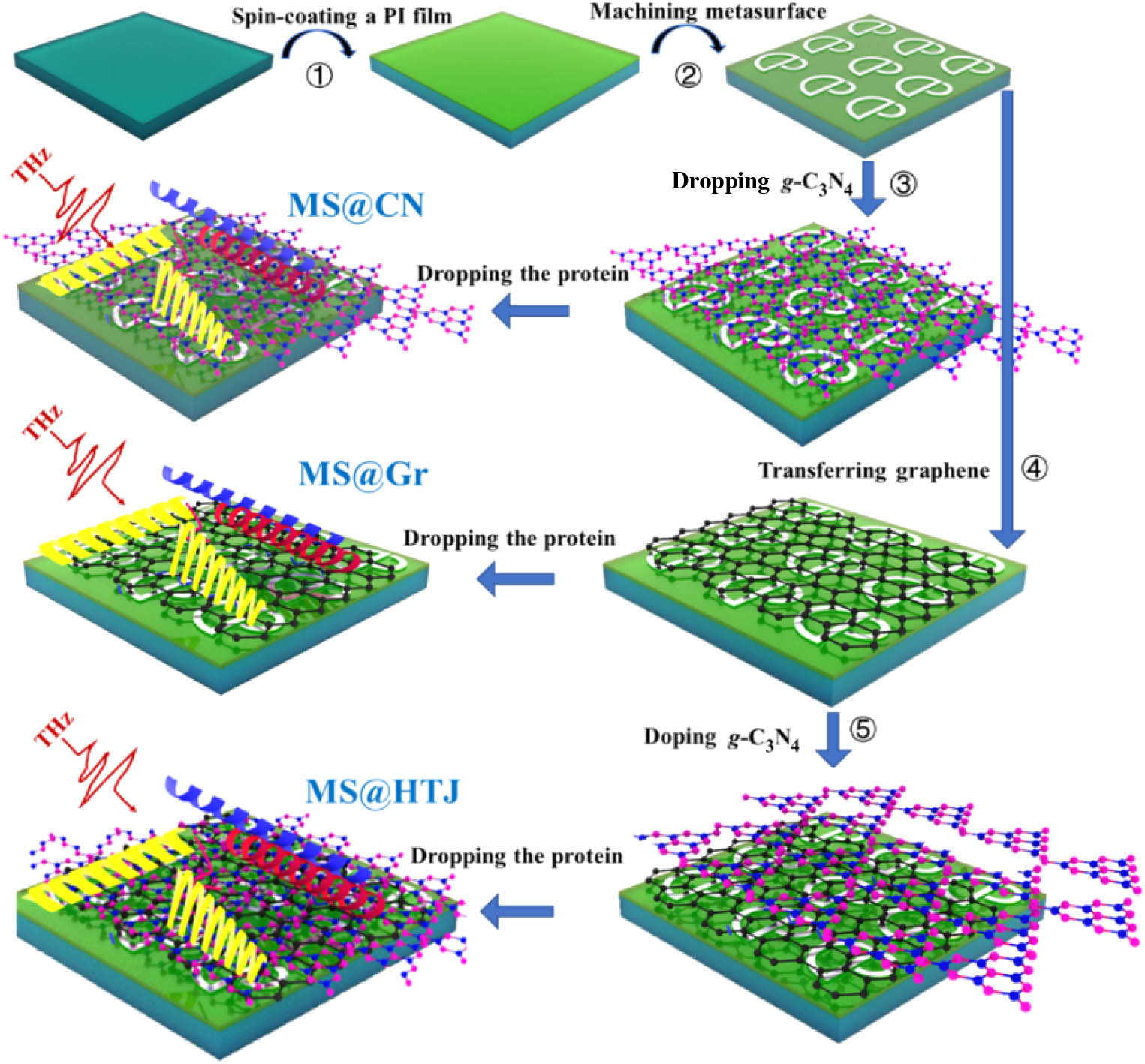
Fig. 1. Schematic illustration of the fabrication of the three proposed biosensors.
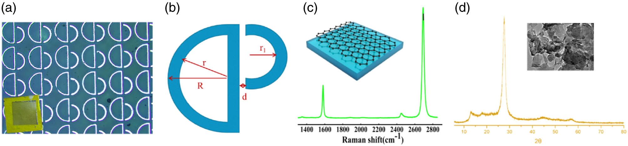
Fig. 2. (a) Photomicrograph of a unit cell of the microstructure. Inset: picture of the sample. (b) Schematic of the unit cell, which consists of D and C shapes. The geometric parameters for D shape are R = 50 μm r = 40 μm r 1 = 20 μm d = 6 μm g - C 3 N 4 g - C 3 N 4
Fig. 3. Left: schematic illustration of three biosensors. Right: simulated and experimental transmission spectrum of the three samples, (a) MS@CN sample, (b) MS@Gr sample, and (c) MS@HTJ sample.
Fig. 4. Simulated and experimental transmission spectrum of the three samples, (a) MS@CN, (b) MS@Gr, and (c) MS@HTJ, respectively.
Fig. 5. Schematic of the energy band structure under different casein concentrations: (a) g - C 3 N 4
Fig. 6. Dependence of (a) frequency and (b) transmission values on protein concentration increasing from 0 to 1.56 ng/mL. Dependence of (c) frequency and (d) transmission difference values on protein concentration increasing from 0 to 1.56 ng/mL.
Fig. 7. Plots of energy bands along the vertical direction from the front surface to the rear surface of (a) g - C 3 N 4 g - C 3 N 4 - graphene Q f E a g - C 3 N 4 C 3 N 4 - graphene Q f Q f = + 10 12 c m − 2 g - C 3 N 4 g - C 3 N 4 - graphene
Fig. 8. Phase difference between the bare sensor (C 0
|
Table 1. Electrical Parameters of Silvaco TCAD Simulation in This Work

Set citation alerts for the article
Please enter your email address
© Copyright 2018-2021 | Chinese Laser Press. All Rights Reserved 沪ICP备15018463号-20