
Weiwei Fu, Kun Huang. All-optical image processing technology and applications based on micro-/nano-devices[J]. Infrared and Laser Engineering, 2020, 49(9): 20201040
- Infrared and Laser Engineering
- Vol. 49, Issue 9, 20201040 (2020)
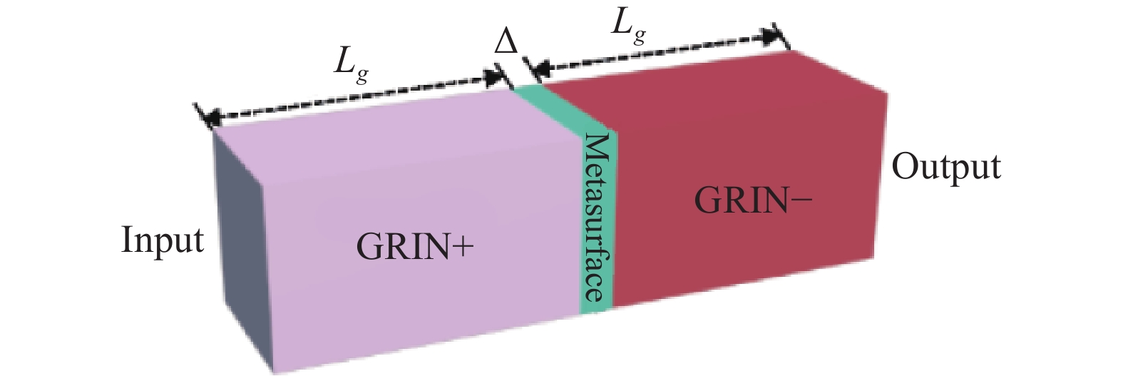
Fig. 1. Wave-based metamaterial computing. A conceptual sketch of a suitably designed metamaterial block that may perform a desired mathematical operation on arbitrary wave signals as they propagate through it. A thin, properly designed metasurfaces sandwiched between two GRIN structures with positive and negative parameters, can perform mathematical operations in the Fourier domain
![Nonlocal metasurface. (a) Schematic of an array of split-ring resonators parallel to the x-z plane. The measurface is excited by TM-polarized waves propagating on the x-z plane; (b) Metasurface with broken x and zsymmetry to obtain an asymmetric response with respect to positive and negative , as required in order to implement a first-derivative operation; (c) Metasurface with a 90° rotational symmetry to implement the second derivative in 2D; (d) Transmission versus incident angle for the metasurface for an second-derivative operation; (e)Transmission versus incidence angle for the metasurface and for an first-derivative operation; (f) Image used to test the response of the metasurface at , where is the resonance frequency of the unmodulated metasurface; (g) Output for illumination (f) with unpolarized light from the normal direction. Panel (a)-(f) adapted with permission from reference [17]非局域超表面。(a) 平行于x-z平面的裂环谐振器阵列示意图。超表面被TM偏振光激发,在x-z平面传播;(b) 设计的超表面对于正和负的打破x和z对称性获取不对称响应,实现一个一阶导数的要求操作;(c) 超表面具有90°旋转对称实现二维的二阶导数;(d) 二阶导数运算的超表面传输与入射角关系;(e) 一阶导数运算的超表面传输与入射角关系;(f) 该图像用于测试在,其中为未调制的超表面的共振频率;(g)法线方向的非偏振光照明图(f)的输出。图(a)~(f)的改动经过参考文献[17]的许可](/richHtml/irla/2020/49/9/20201040/img_2.jpg)
Fig. 2. Nonlocal metasurface. (a) Schematic of an array of split-ring resonators parallel to the x -z plane. The measurface is excited by TM-polarized waves propagating on the x -z plane; (b) Metasurface with broken x and z symmetry to obtain an asymmetric response with respect to positive and negative
, as required in order to implement a first-derivative operation; (c) Metasurface with a 90° rotational symmetry to implement the second derivative in 2D; (d) Transmission versus incident angle for the metasurface for an second-derivative operation; (e)Transmission versus incidence angle for the metasurface and for an first-derivative operation; (f) Image used to test the response of the metasurface at
, where
is the resonance frequency of the unmodulated metasurface; (g) Output for illumination (f) with unpolarized light from the normal direction. Panel (a)-(f) adapted with permission from reference [17]
非局域超表面。(a) 平行于x-z 平面的裂环谐振器阵列示意图。超表面被TM偏振光激发,在x-z 平面传播;(b) 设计的超表面对于正和负的
打破x 和z 对称性获取不对称响应,实现一个一阶导数的要求操作;(c) 超表面具有90°旋转对称实现二维的二阶导数;(d) 二阶导数运算的超表面传输与入射角关系;(e) 一阶导数运算的超表面传输与入射角关系;(f) 该图像用于测试在
,其中
为未调制的超表面的共振频率;(g)法线方向的非偏振光照明图(f)的输出。图(a)~(f)的改动经过参考文献[17]的许可
Fig. 3. Design of surface-plasmon-based spatial differentiator. (a) Schematic of the plasmonic spatial differentiator with the Kretschmann configuration to excite the surface plasmon polariton(SPP). The dark grey layer and the light grey area correspond to the silver film and the glass, respectively; (b)-(d) Spatial transfer function spectra of the three samples by the experimental measurement (dotted lines) and the numerical fitting (solid lines). In the numerical calculation, the thicknesses of the silver layer were 46.0 nm, 50.0 nm and 55.5 nm, respectively.
corresponds to the incident angle for the phase matching; (e) Left: incident image consisting of the Stanford tree logo and letters generated with phase modulation, where the inside and the outside of the letters and the logo have different phases but the same intensity. Right: reflected intensity image. (f) Left: incident image consisting of the ZJU eagle logo and letters with amplitude modulation where the inside and the outside of the letters and the eagle have different intensities. Right: reflected intensity image. Scale bar:100 μm. Panel (a)-(f) adapted with permission from reference [19]基于表面等离子体的空间微分器设计。(a) 利用Kretschmann 装置激发表面等离子体极化子(SPP)的等离子体空间微分器的原理图。深灰色层和浅灰色区域分别对应于银膜和玻璃;(b)~(d) 通过实验测量(虚线)和数值拟合(实线)得到三个样本的空间传递函数谱。在数值计算中,银层厚度分别为46.0 nm、50.0 nm和55.5 nm。
对应相位匹配的入射角;(e) 左边:相位调制产生的斯坦福标志字母组成入射图像相对应的反射强度图像,其中字母和标志的内外具有不同的相位,但强度相同;右边:反射强度图像。(f) 左边:由字母“ZJU”和“鹰”标志组成的入射图像,其中“字母”标志的内外与“鹰”标志的强度不同;右边:反射强度图像。比例尺:100 μm。图(a)~(f)的改动经过参考文献[19]的许可
Fig. 4. Photonic crystal slab differentiator. (a) Geometry of the photonic crystal slab differentiator, which consists of a photonic crystal slab separated from a uniform dielectric slab by an air gap. For
, the geometry parameters are:
,
,
,
, where a is the lattice constant; (b) Coordinate system; (c) Brillouin zone of the system; Contour plots of transmittance
as a function of
and
at frequency
for (d) S light
, (e) P light
, and (f) unpolarized light
, which are all isotropic near Γ; (g)
as a function of
along the φ =14° direction, and the quadratic fitting
where
is the only fitting parameter; (h) Incident Stanford emblem with a size of 2 610 a × 1 729S 光
,(e)P 光
, 和(f)无偏振光
,这些都是各向同性Γ附近;(g) 沿着φ =14°方向
作为
函数,二次拟合
,
是仅有的拟合参数;(h) 小为2 610a ×1 729a的Stanford徽章;(i) 计算传输的无偏振光图像,清晰显示不同方向的边缘。图(a)~(h)的改动经过参考文献[18]的许可
Fig. 5. Two-dimensional image differentiation using nanophotonic materials. Schematic of a photonic crystal slab acting as a Laplacian operator that transforms an image,
, into its second-order derivative,
. The unit cell of the differentiator is composed of Si nanorods
使用纳米光子材料的二维图像微分。光子晶体板作为拉普拉斯操作变换图像
生成其二阶微分
的示意图,微分器的单元由硅纳米棒组成
Fig. 6. Spiral phase differentiator. (a) Schematic of the designed all-dielectric metasurface spatial filter. Inset: perspective and top view of the metasurface unit-cell formed by amorphous TiO2nanopillar sitting on a silica substrate; (b) Optical photograph of the fabricated metasurface device. Scale bar: 500 μm; (c) Top view and oblique view of the SEM images of TiO2nanopillar array. Scale bars: 1 μm; (d) Sketch of the experimental setup for spin-dependent spiral phase contrast imaging. LP and QWP can make the incident light with circular polarization. CP can be used to eliminate background light in the optical path. (e)-(h) Traditional bright-field images captured with LCP incident light at the wavelength of 480, 530, 580, 630 nm, respectively; (i)-(l) Spiral phase contrast images captured with RCP incident light at the corresponding wavelengths. Scale bar:100 μm. Panel 6(a)-6(l) adapted with permission from reference [42]
Fig. 7. Principle of QPGM-based differentiator. Schematic of the QPGM employing two metasurface layers, where the second layer is composed of three separate metasurface lenses. The first metasurface, together with each of the lenses in the second metasurface layer. Metasurface 1 makes two sheared focuses for TE and TM polarizations and splits the field in three different directions towards the three lenses in the second layer. With the polarizer, the three metasurface lenses in layer 2 form three DIC images (
,
and
) having different phase offsets between the TE and TM polarizations
基于QGPM微分器的原理。采用两个超表面层的QPGM原理图,第二层由三个独立的超表面透镜组成。第一超表面与第二超表面层中的每一个透镜一起,超表面一对TE和TM偏振产生两个剪切聚焦,并将场向三个不同的方向向着第二层的三个透镜。在偏振片下,第二层的三个超表面透镜形成三个DIC图像(
,
和
),在TE和TM偏振之间有不同的相位偏移
Fig. 8. Differentiator based PB phase. (a) Photograph of a 1 in (1 in=2.54 cm) diameter sample. Metasurface patterned area, 8 mm × 8 mm (scale bar:5 mm); (b) Polariscope optical image of the sample pattern area marked in (a). The red bars indicate structures orientation in one period. (Inset) SEM image of the induced nanostructure(Scale bar: 500 nm); (c) Experimental setup: The incident light then passes through the object, which is followed by a 4f system. The sample (metasurface) is placed in between of the P1 and P2. L: lens, P: polarizer; (d)-(f) The first row shows images without the analyzer; the illumination wavelengths are 430 nm, 500 nm, and 670 nm, respectively. The images are taken with metasurface period Λ of 8,000 μm. The second row shows resultant images after adding an analyzer. Panel 8(a)-8(f) adapted with permission from reference [44]
Fig. 9. Differentiator based SHE. (a) Schematic of spatial differentiation from the SHE of light on an optical planar interface between two isotropic materials, e.g., an air-glass interface; (b)-(c) Measured intensity profiles of the incident and reflected beams, respectively; (d) Incident image consisting of the Chinese character for “light” with amplitude modulation on
; (e) Reflected intensity image corresponding to (d) by measuring
. Scale bar: 50 μm. Panel 9(a)-(e) adapted with permission from reference [46]
基于自旋霍尔效应的微分器。(a) 两种各向同性材料(如空气-玻璃界面)由于光的SHE在光学平面界面上的空间微分示意图。(b)~(c)分别测量的入射和反射光束的强度分布图;(d) 入射图像由汉字“光”振幅图像
;(e) 测量
对应于(d)的反射强度图像。比例尺:50 μm。图9(a)~(e)的改动经过参考文献[46]的许可

Set citation alerts for the article
Please enter your email address
© Copyright 2018-2021 | Chinese Laser Press. All Rights Reserved 沪ICP备15018463号-20