• Photonics Research
  • Vol. 7, Issue 2, 201 (2019)
Riccardo Marchetti1, Cosimo Lacava2、*, Lee Carroll3, Kamil Gradkowski3, and Paolo Minzioni1
Author Affiliations
  • 1Electrical, Computer and Biomedical Engineering Department, University of Pavia, Pavia 27100, Italy
  • 2Optoelectronics Research Centre, Highfield Campus, University of Southampton, Southampton SO17 1BJ, UK
  • 3Photonic Packaging Group, Tyndall National Institute, Lee Maltings Complex, Cork T12R5CP, Ireland
  • show less
    DOI: 10.1364/PRJ.7.000201 Cite this Article Set citation alerts
    Riccardo Marchetti, Cosimo Lacava, Lee Carroll, Kamil Gradkowski, Paolo Minzioni. Coupling strategies for silicon photonics integrated chips [Invited][J]. Photonics Research, 2019, 7(2): 201 Copy Citation Text show less
    Conceptual organization of the different structures proposed for optical coupling and discussed in the present text.
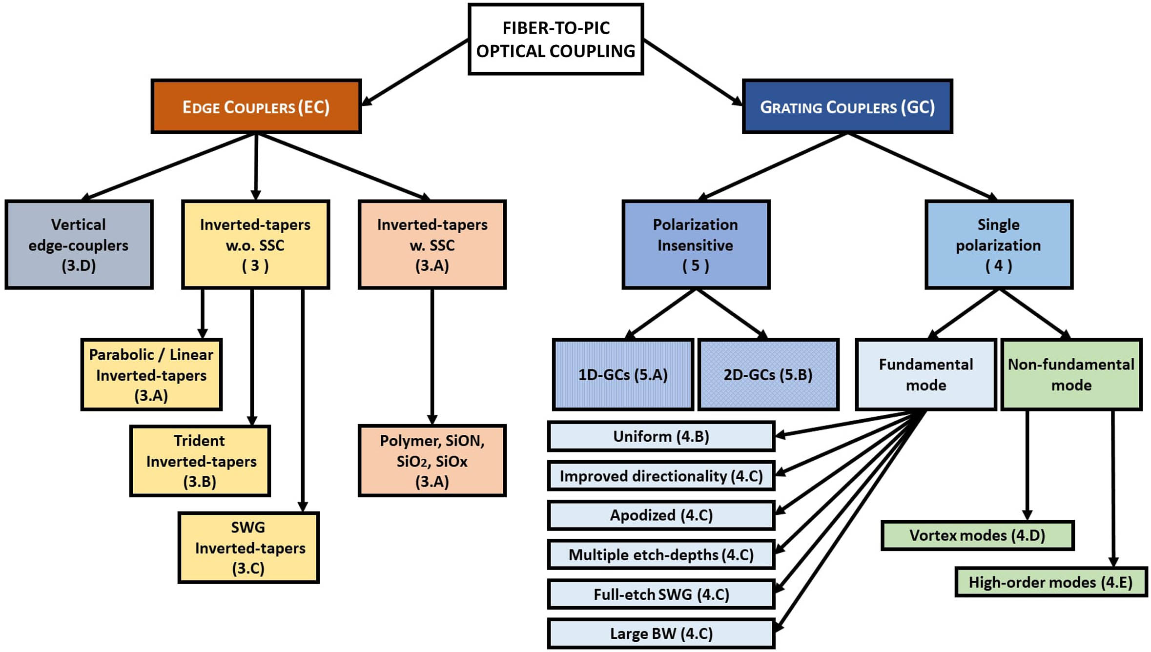
    Fig. 1. Conceptual organization of the different structures proposed for optical coupling and discussed in the present text.
    (a) Cross-section schematic of an SMF28 fiber, showing the 8.2 μm fiber core centered in the cladding layer, wave-guiding the 10.4 μm MFD 1.55 μm mode. Side view schematics of (b) planar polished, (c) angle polished, and (d) lensed SMF28. (e) Schematic of UHNA-to-SMF28 splicing, showing the thermally expanded adiabatic taper. The (b), (d), and (e) geometries are commonly used for edge coupling, while the (c) geometry is preferred for grating coupling.
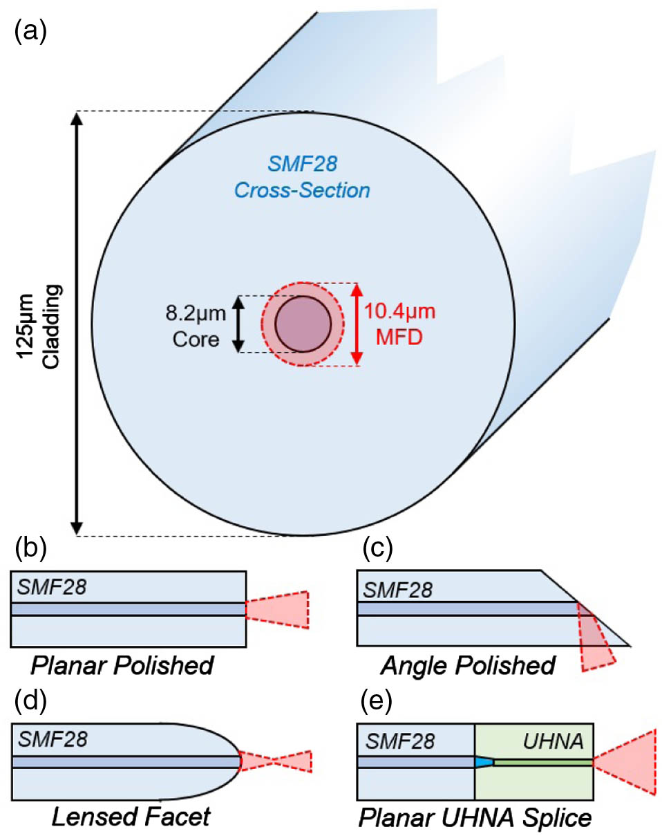
    Fig. 2. (a) Cross-section schematic of an SMF28 fiber, showing the 8.2 μm fiber core centered in the cladding layer, wave-guiding the 10.4 μm MFD 1.55 μm mode. Side view schematics of (b) planar polished, (c) angle polished, and (d) lensed SMF28. (e) Schematic of UHNA-to-SMF28 splicing, showing the thermally expanded adiabatic taper. The (b), (d), and (e) geometries are commonly used for edge coupling, while the (c) geometry is preferred for grating coupling.
    Schematic of a standard SOI EC for coupling light between an SOI waveguide and a tapered single-mode fiber. The waveguide (WG) is tapered down to a small tip to allow mode expansion in the horizontal direction, whereas an overlay of polymer, Si3N4, SiON, or SiOx, is deposited over the taper, to allow mode expansion in the vertical direction.
    Fig. 3. Schematic of a standard SOI EC for coupling light between an SOI waveguide and a tapered single-mode fiber. The waveguide (WG) is tapered down to a small tip to allow mode expansion in the horizontal direction, whereas an overlay of polymer, Si3N4, SiON, or SiOx, is deposited over the taper, to allow mode expansion in the vertical direction.
    (a) SEM image of the optical facet and edge-coupler region on an SOI-PIC, showing the mirror-finish optical facet, deeper RIE trench for fiber access, and the diced edge of the PIC for singulation from the rest of the wafer. (b) Schematic of a multichannel fiber array, showing the 250 μm pitched array of fibers sandwiched between a V-groove array and a contact plate.
    Fig. 4. (a) SEM image of the optical facet and edge-coupler region on an SOI-PIC, showing the mirror-finish optical facet, deeper RIE trench for fiber access, and the diced edge of the PIC for singulation from the rest of the wafer. (b) Schematic of a multichannel fiber array, showing the 250 μm pitched array of fibers sandwiched between a V-groove array and a contact plate.
    Schematic of the SOI edge-coupling structure proposed in [31], based on the use of a double-layer Si inverse taper and a SiO2 waveguide. Reproduced from [31].
    Fig. 5. Schematic of the SOI edge-coupling structure proposed in [31], based on the use of a double-layer Si inverse taper and a SiO2 waveguide. Reproduced from [31].
    Schematic of the SOI edge-coupling structure proposed in [32], based on the use of a Si inverse taper and a SiO2 waveguide implemented in the BOX. A V-groove is etched in the Si substrate to allow for fiber auto-alignment. Reproduced from [32].
    Fig. 6. Schematic of the SOI edge-coupling structure proposed in [32], based on the use of a Si inverse taper and a SiO2 waveguide implemented in the BOX. A V-groove is etched in the Si substrate to allow for fiber auto-alignment. Reproduced from [32].
    (top) Schematic of the SOI trident EC structure proposed in [33]. Reproduced from [34]. (bottom) Top view of the trident SOI EC structure proposed in [33].
    Fig. 7. (top) Schematic of the SOI trident EC structure proposed in [33]. Reproduced from [34]. (bottom) Top view of the trident SOI EC structure proposed in [33].
    SEM image of an SWG waveguide. Inset shows the dispersion diagrams (for TE polarization) of an SWG waveguide (blue curve) and of a standard strip waveguide (red curve) having an effective refractive index of 2.65. The two curves show a good match when away from the bandgap resonance. Reproduced from [36].
    Fig. 8. SEM image of an SWG waveguide. Inset shows the dispersion diagrams (for TE polarization) of an SWG waveguide (blue curve) and of a standard strip waveguide (red curve) having an effective refractive index of 2.65. The two curves show a good match when away from the bandgap resonance. Reproduced from [36].
    (a) Schematic representation of the SWG-based EC described in [37]. (b) SEM image of the fabricated SWG-based EC. Reproduced from [37].
    Fig. 9. (a) Schematic representation of the SWG-based EC described in [37]. (b) SEM image of the fabricated SWG-based EC. Reproduced from [37].
    Schematic representation of the EC structure optimized for a 10.4 μm MFD, presented in [39]. A ridge waveguide is formed in the upper cladding over the Si inverse taper, and Si3N4 layers are deposited in order to increase the effective refractive index of the upper cladding. The dimensions are not to scale.
    Fig. 10. Schematic representation of the EC structure optimized for a 10.4 μm MFD, presented in [39]. A ridge waveguide is formed in the upper cladding over the Si inverse taper, and Si3N4 layers are deposited in order to increase the effective refractive index of the upper cladding. The dimensions are not to scale.
    Fundamental TE mode distribution at the coupler tip, of the structure optimized for a 10.4 μm MFD. The mode is pulled toward the upper cladding, therefore overcoming optical leakage to the Si substrate. Reproduced from [39].
    Fig. 11. Fundamental TE mode distribution at the coupler tip, of the structure optimized for a 10.4 μm MFD. The mode is pulled toward the upper cladding, therefore overcoming optical leakage to the Si substrate. Reproduced from [39].
    SEM image of a vertically bent optical coupler, obtained by ion implantation in a silicon waveguide. The bent waveguide is 5 μm long, and the curvature radius is approximately equal to 3 μm. Reproduced from [43].
    Fig. 12. SEM image of a vertically bent optical coupler, obtained by ion implantation in a silicon waveguide. The bent waveguide is 5 μm long, and the curvature radius is approximately equal to 3 μm. Reproduced from [43].
    Schematic representation of a 1D-GC used as an outcoupling device. Si layer thickness, BOX layer, etched depth, and fiber core are shown with the right relative proportions.
    Fig. 13. Schematic representation of a 1D-GC used as an outcoupling device. Si layer thickness, BOX layer, etched depth, and fiber core are shown with the right relative proportions.
    Cross-sectional schematic of a uniform GC implemented in SOI technology.
    Fig. 14. Cross-sectional schematic of a uniform GC implemented in SOI technology.
    Wave-vector diagrams of waveguide GCs in resonant configuration.
    Fig. 15. Wave-vector diagrams of waveguide GCs in resonant configuration.
    Wave-vector diagrams of waveguide GCs in detuned configuration.
    Fig. 16. Wave-vector diagrams of waveguide GCs in detuned configuration.
    (a) Schematic top view of a GC with straight trenches. (b) Schematic top view of a focusing GC.
    Fig. 17. (a) Schematic top view of a GC with straight trenches. (b) Schematic top view of a focusing GC.
    (Top) CE for a UGC implemented in a standard SOI platform (S=220 nm and B=2000 nm), with a grating period Λ=634 nm and FF=0.5. CE is reported as a function of optical wavelength λ for different values of etching depth e, ranging from 60 to 80 nm. (Bottom) CE for a UGC implemented in a standard SOI platform (S=220 nm and B=2000 nm), with a grating period Λ=634 nm and e=70 nm. CE is reported as a function of optical wavelength λ for different values of FF, ranging from 0.4 to 0.6.
    Fig. 18. (Top) CE for a UGC implemented in a standard SOI platform (S=220  nm and B=2000  nm), with a grating period Λ=634  nm and FF=0.5. CE is reported as a function of optical wavelength λ for different values of etching depth e, ranging from 60 to 80 nm. (Bottom) CE for a UGC implemented in a standard SOI platform (S=220  nm and B=2000  nm), with a grating period Λ=634  nm and e=70  nm. CE is reported as a function of optical wavelength λ for different values of FF, ranging from 0.4 to 0.6.
    CE of a TE-optimized 1D-GC as a function of optical wavelength for TE light polarization (blue trace) and for TM light polarization (red trace).
    Fig. 19. CE of a TE-optimized 1D-GC as a function of optical wavelength for TE light polarization (blue trace) and for TM light polarization (red trace).
    Normalized power density profile of the diffracted mode from a UGC, implemented in a 220 nm Si thick SOI platform with a 70 nm deep etch.
    Fig. 20. Normalized power density profile of the diffracted mode from a UGC, implemented in a 220 nm Si thick SOI platform with a 70 nm deep etch.
    Normalized power density profile of the diffracted mode from UGCs, implemented in 220 nm Si thick SOI platform with a 70 nm etch depth and FF ranging from 0.5 to 0.8.
    Fig. 21. Normalized power density profile of the diffracted mode from UGCs, implemented in 220 nm Si thick SOI platform with a 70 nm etch depth and FF ranging from 0.5 to 0.8.
    Schematic of the SOI-blazed GC proposed in [57].
    Fig. 22. Schematic of the SOI-blazed GC proposed in [57].
    Schematic of the 1D-GC structure proposed in [58]. Good CE is obtained thanks to the presence of an aluminum layer deposited in the region above the GC.
    Fig. 23. Schematic of the 1D-GC structure proposed in [58]. Good CE is obtained thanks to the presence of an aluminum layer deposited in the region above the GC.
    Gaussian output beam and corresponding α(z) calculated according to Eq. (14). Dotted curve is the resulting output from the simulation after numerical optimization. Reproduced from [59].
    Fig. 24. Gaussian output beam and corresponding α(z) calculated according to Eq. (14). Dotted curve is the resulting output from the simulation after numerical optimization. Reproduced from [59].
    CE of the optimized nonuniform SOI GC proposed in [59], with (continuous line) and without (dashed line) of a two-pair DBR. Reproduced from [59].
    Fig. 25. CE of the optimized nonuniform SOI GC proposed in [59], with (continuous line) and without (dashed line) of a two-pair DBR. Reproduced from [59].
    Schematic structure of the DBR-assisted UGC reported in [60].
    Fig. 26. Schematic structure of the DBR-assisted UGC reported in [60].
    Schematic structure of the Au-mirror-assisted UGC reported in [62].
    Fig. 27. Schematic structure of the Au-mirror-assisted UGC reported in [62].
    Schematic structure of the poly-Si overlayer UGC reported in [65].
    Fig. 28. Schematic structure of the poly-Si overlayer UGC reported in [65].
    Schematic structure of the Si-nmb overlayer UGC reported in [68].
    Fig. 29. Schematic structure of the Si-nmb overlayer UGC reported in [68].
    Schematic representation of a slanted SOI GC. The period of the uniform grating is equal to Λ and the etched slits angle is equal to δ.
    Fig. 30. Schematic representation of a slanted SOI GC. The period of the uniform grating is equal to Λ and the etched slits angle is equal to δ.
    Cross-sectional schematic of a nonuniform GC implemented in an SOI wafer, based on a linear apodization of the grating FF.
    Fig. 31. Cross-sectional schematic of a nonuniform GC implemented in an SOI wafer, based on a linear apodization of the grating FF.
    Maximum CE at λ=1.55 μm for the linear AGC based on 220 nm SOI (red plot) and 260 nm SOI (blue plot). Reproduced from [76].
    Fig. 32. Maximum CE at λ=1.55  μm for the linear AGC based on 220 nm SOI (red plot) and 260 nm SOI (blue plot). Reproduced from [76].
    GC directionality, at λ=1.55 μm, as a function of e for the linearly apodized grating (green curve) and for a uniform grating configuration (purple curve). Reproduced from [76].
    Fig. 33. GC directionality, at λ=1.55  μm, as a function of e for the linearly apodized grating (green curve) and for a uniform grating configuration (purple curve). Reproduced from [76].
    Efficiency comparison between optimized uniform grating designs (black line and squares) and optimized apodized grating designs (red and blue lines and symbols) as functions of the SOI thickness. The red curve with dots refers to apodized gratings obtained from an FF linear chirp and genetic algorithm optimization, while the blue curve with triangles refers to those obtained by optimizing the structure reported in [46]. The theoretical CE of the record-efficiency design for a 1D-GC with an Al backreflector ([63]) is denoted with a dashed horizontal black line. The CE of the apodized design with deep-UV lithographic constraints (minimum feature = 100 nm) is denoted with an open green square. Adapted from [75].
    Fig. 34. Efficiency comparison between optimized uniform grating designs (black line and squares) and optimized apodized grating designs (red and blue lines and symbols) as functions of the SOI thickness. The red curve with dots refers to apodized gratings obtained from an FF linear chirp and genetic algorithm optimization, while the blue curve with triangles refers to those obtained by optimizing the structure reported in [46]. The theoretical CE of the record-efficiency design for a 1D-GC with an Al backreflector ([63]) is denoted with a dashed horizontal black line. The CE of the apodized design with deep-UV lithographic constraints (minimum feature = 100 nm) is denoted with an open green square. Adapted from [75].
    Schematic cross-section of a UGC implemented with the double-etch technique reported in [77]. ϕh and ϕv, respectively, represent the horizontal and vertical phase shift between two consecutive grating trenches.
    Fig. 35. Schematic cross-section of a UGC implemented with the double-etch technique reported in [77]. ϕh and ϕv, respectively, represent the horizontal and vertical phase shift between two consecutive grating trenches.
    Schematic representation of the multi-etch GC proposed in [81], where the lag effect of ICP-RIE is exploited.
    Fig. 36. Schematic representation of the multi-etch GC proposed in [81], where the lag effect of ICP-RIE is exploited.
    Schematic representation of a nano-hole GC designed for a coupling angle θ of 8°.
    Fig. 37. Schematic representation of a nano-hole GC designed for a coupling angle θ of 8°.
    (Left) Top view of the grating based on a nano-hole array. (Right) 2D model of the waveguide grating with a nano-hole array based on a slab structure.
    Fig. 38. (Left) Top view of the grating based on a nano-hole array. (Right) 2D model of the waveguide grating with a nano-hole array based on a slab structure.
    (Top) Cross-sectional schematic of the Si3N4 GC proposed in [95]. The access waveguide thickness (t) is equal to thickness of the native Si3N4 layer (tSN) minus the etch depth (tg). (Bottom) Schematic top view of the focusing GC structure proposed in [95], where an inverse taper was used to connect the grating section and the Si3N4 strip waveguides. The optimized geometrical parameters are Wt=150 nm, We=4 μm, Wg=900 nm, and Lt=20 μm.
    Fig. 39. (Top) Cross-sectional schematic of the Si3N4 GC proposed in [95]. The access waveguide thickness (t) is equal to thickness of the native Si3N4 layer (tSN) minus the etch depth (tg). (Bottom) Schematic top view of the focusing GC structure proposed in [95], where an inverse taper was used to connect the grating section and the Si3N4 strip waveguides. The optimized geometrical parameters are Wt=150  nm, We=4  μm, Wg=900  nm, and Lt=20  μm.
    Perspective representation of the Si3N4-on-SOI dual-level GC reported in [97]. Reproduced from [97].
    Fig. 40. Perspective representation of the Si3N4-on-SOI dual-level GC reported in [97]. Reproduced from [97].
    Cross-sectional schematic of the Si3N4-on-SOI dual-level GC reported in [98]. Reproduced from [98].
    Fig. 41. Cross-sectional schematic of the Si3N4-on-SOI dual-level GC reported in [98]. Reproduced from [98].
    GC forked design for vortex beam optical mode. Reproduced from [103].
    Fig. 42. GC forked design for vortex beam optical mode. Reproduced from [103].
    (a) Schematic of a GC excited either with a TE00 (blue) or TE10 (red) waveguide mode. (Inset) Field plot of a scattered TE10 mode. (b) Effective refractive indices of the first three guided modes in an SOI nanowire of height 220 nm at λ=1.55 μm. (c) Cross-section of the scattered electric field profiles of a standard GC excited from both ends with Δφ=0° (blue) and Δφ=180° (red). Reproduced from [107]. This device can be used to simultaneously couple different fiber spatial modes to silicon photonic multimode waveguides.
    Fig. 43. (a) Schematic of a GC excited either with a TE00 (blue) or TE10 (red) waveguide mode. (Inset) Field plot of a scattered TE10 mode. (b) Effective refractive indices of the first three guided modes in an SOI nanowire of height 220 nm at λ=1.55  μm. (c) Cross-section of the scattered electric field profiles of a standard GC excited from both ends with Δφ=0° (blue) and Δφ=180° (red). Reproduced from [107]. This device can be used to simultaneously couple different fiber spatial modes to silicon photonic multimode waveguides.
    LP11 GC structure proposed by [108]. Reproduced from [108].
    Fig. 44. LP11 GC structure proposed by [108]. Reproduced from [108].
    Structure proposed by [110] to excite the LP11b mode from a silicon photonic single-mode waveguide.
    Fig. 45. Structure proposed by [110] to excite the LP11b mode from a silicon photonic single-mode waveguide.
    Schematic of the designed strategy proposed in [111] to obtain a polarization insensitive 1D-GC. Grating (a) is obtained by the geometrical intersection of two different UGCs, having a grating period optimized for TE and TM light polarization, respectively. Grating (b) is obtained by the union of the same two UGCs. Reproduced from [111].
    Fig. 46. Schematic of the designed strategy proposed in [111] to obtain a polarization insensitive 1D-GC. Grating (a) is obtained by the geometrical intersection of two different UGCs, having a grating period optimized for TE and TM light polarization, respectively. Grating (b) is obtained by the union of the same two UGCs. Reproduced from [111].
    Cross-sectional schematic of the GC proposed in [112].
    Fig. 47. Cross-sectional schematic of the GC proposed in [112].
    (a) Schematic of a 2D grating-coupler (2D-GC) on the SOI photonic platform, showing the angle-of-incidence (θ) and the polarization angle (φ) of the incident fiber mode. Inset shows the definition of the pitch (P) and radius (R) of the partially etched cylinders making up the 2D-GC. (b) The coupling efficiency into the two orthogonal arms (in the x and y directions) of the 2D-GC as a function of the polarization angle. Adapted from [117].
    Fig. 48. (a) Schematic of a 2D grating-coupler (2D-GC) on the SOI photonic platform, showing the angle-of-incidence (θ) and the polarization angle (φ) of the incident fiber mode. Inset shows the definition of the pitch (P) and radius (R) of the partially etched cylinders making up the 2D-GC. (b) The coupling efficiency into the two orthogonal arms (in the x and y directions) of the 2D-GC as a function of the polarization angle. Adapted from [117].
    (a) Schematic of a 2D grating-coupler (2D-GC) with long adiabatic taper waveguides to match the SMF28 coupled mode to the dimensions of the SOI waveguide (i.e., 450 nm×220 nm). (b) A large 3D-FDTD simulation (75 μm×25 μm) is used to illustrate the slight angular offset between the direction of coupled-mode propagation and the symmetry axis of the 2D-GC. Adapted from [117].
    Fig. 49. (a) Schematic of a 2D grating-coupler (2D-GC) with long adiabatic taper waveguides to match the SMF28 coupled mode to the dimensions of the SOI waveguide (i.e., 450  nm×220  nm). (b) A large 3D-FDTD simulation (75  μm×25  μm) is used to illustrate the slight angular offset between the direction of coupled-mode propagation and the symmetry axis of the 2D-GC. Adapted from [117].
    Dependence of CEx, CEy, and CET on the input-beam polarization angle. Adapted from [117].
    Fig. 50. Dependence of CEx, CEy, and CET on the input-beam polarization angle. Adapted from [117].
    CE contour plot at λ=1.55 μm as a function of E and R/P for a 2D-GC realized on the SOI platform with S=220 nm. The optimum performance corresponds to E=120 nm and R/P=0.3. Reproduced from [117].
    Fig. 51. CE contour plot at λ=1.55  μm as a function of E and R/P for a 2D-GC realized on the SOI platform with S=220  nm. The optimum performance corresponds to E=120  nm and R/P=0.3. Reproduced from [117].
    (a) Schematic showing that a nominally “full” etch provides only partial etching for small sub-λ features. (b) Layout of the sub-λ cluster that acts as a unified scattering site for the 2D-GC. (c) The periodic layout of the sub-λ clusters to create the 2D-GC.
    Fig. 52. (a) Schematic showing that a nominally “full” etch provides only partial etching for small sub-λ features. (b) Layout of the sub-λ cluster that acts as a unified scattering site for the 2D-GC. (c) The periodic layout of the sub-λ clusters to create the 2D-GC.
    (a) Periodic layout of the asymmetric clusters used to realize a 2D-GC with reduced polarization dependent loss (PDL). (b) and (c) Detail of the tuned clusters, showing the asymmetric dS and dP spacing of the different subcylinders etched into the SOI layer. The optimum design parameters are dP=250 nm, dS=360 nm, E=70 nm, R=200 nm, and P=612 nm.
    Fig. 53. (a) Periodic layout of the asymmetric clusters used to realize a 2D-GC with reduced polarization dependent loss (PDL). (b) and (c) Detail of the tuned clusters, showing the asymmetric dS and dP spacing of the different subcylinders etched into the SOI layer. The optimum design parameters are dP=250  nm, dS=360  nm, E=70  nm, R=200  nm, and P=612  nm.
    Schematic of an end-to-end photonic-circuit with an identical 2D-GC for both the input and output optical interconnects. (a) In the initial scheme, the input mode and the output mode both have the same polarization angle, i.e., φin=φout, so the end-to-end transmission exhibits twice the polarization dependence of a single 2D-GC, i.e., PDL(φin)·PDL(φout)=PDL2(φin). (b) In the π shift scheme, the polarization states of the input and output modes are rotated such that the maximum and minimum of PDL(φin) from the input 2D-GC are anticorrelated with PDL(φout), so that PDL(φin)·PDL(φout)=0.
    Fig. 54. Schematic of an end-to-end photonic-circuit with an identical 2D-GC for both the input and output optical interconnects. (a) In the initial scheme, the input mode and the output mode both have the same polarization angle, i.e., φin=φout, so the end-to-end transmission exhibits twice the polarization dependence of a single 2D-GC, i.e., PDL(φin)·PDL(φout)=PDL2(φin). (b) In the π shift scheme, the polarization states of the input and output modes are rotated such that the maximum and minimum of PDL(φin) from the input 2D-GC are anticorrelated with PDL(φout), so that PDL(φin)·PDL(φout)=0.
    (a) Schematic of the wafer-level postprocessing steps used to deposit a metal (or DBR) bottom reflector beneath a 2D-GC to enhance the fiber-to-PIC CE. (b) Contour plot of 1.55 μm CE as a function of etch-to-thickness ratio (E/S) and radius-to-pitch ratio (R/P) for a 160 nm thick SOI-PIC with a BOX layer thickness of 2175 nm. Adapted from [120].
    Fig. 55. (a) Schematic of the wafer-level postprocessing steps used to deposit a metal (or DBR) bottom reflector beneath a 2D-GC to enhance the fiber-to-PIC CE. (b) Contour plot of 1.55 μm CE as a function of etch-to-thickness ratio (E/S) and radius-to-pitch ratio (R/P) for a 160 nm thick SOI-PIC with a BOX layer thickness of 2175 nm. Adapted from [120].
    Alignment tolerances for (a) 10.4 μm MFD GC and (b) 3.5 μm MFD EC.
    Fig. 56. Alignment tolerances for (a) 10.4 μm MFD GC and (b) 3.5 μm MFD EC.
    Finding first light during alignment. (a) FA is far away from the PIC leading to weak albeit wide signal. (b) Optimized distance between FA and PIC leads to a strong, narrow Gaussian beam shape. (c) Using red light to align the fiber to the EC. Scattering is observed as the waveguide turns 90°.
    Fig. 57. Finding first light during alignment. (a) FA is far away from the PIC leading to weak albeit wide signal. (b) Optimized distance between FA and PIC leads to a strong, narrow Gaussian beam shape. (c) Using red light to align the fiber to the EC. Scattering is observed as the waveguide turns 90°.
    Schematic effects of epoxy shrinkage on coupling interface. Black elements represent the PIC, the submount is indicated in gray, the fiber (or FA) is reported in blue, yellow is the mechanical epoxy, and green is the optical epoxy. Red arrows show the direction of the force during shrinkage. (a) GC, notice that optical epoxy also plays a mechanical role. (b) Single fiber. (c) FA attached directly to PIC submount. (d) FA attached to PIC submount through its own. Panels (e) and (f) show a practical realization of package designs in (b) and (d), respectively.
    Fig. 58. Schematic effects of epoxy shrinkage on coupling interface. Black elements represent the PIC, the submount is indicated in gray, the fiber (or FA) is reported in blue, yellow is the mechanical epoxy, and green is the optical epoxy. Red arrows show the direction of the force during shrinkage. (a) GC, notice that optical epoxy also plays a mechanical role. (b) Single fiber. (c) FA attached directly to PIC submount. (d) FA attached to PIC submount through its own. Panels (e) and (f) show a practical realization of package designs in (b) and (d), respectively.
    Zemax Gaussian beam propagation simulations of packages utilizing micro-optics. (a) Collimation of six beams from GCs. (b) Micro-optical bench. (c) Pluggable free-space coupler.
    Fig. 59. Zemax Gaussian beam propagation simulations of packages utilizing micro-optics. (a) Collimation of six beams from GCs. (b) Micro-optical bench. (c) Pluggable free-space coupler.
    Picture of a package exploiting the μ-lens-assisted pluggable connector described in [131]. A pair of lenses (highlighted) are attached to the FA and the PIC. Adapted from [131].
    Fig. 60. Picture of a package exploiting the μ-lens-assisted pluggable connector described in [131]. A pair of lenses (highlighted) are attached to the FA and the PIC. Adapted from [131].
    (a) Schematic of free-space fiber-to-PIC coupling using a single μ-lens. Here, the mode emitted by the edge coupler is weakly focused by a μ-lens to give a 10 μm MFD mode size and NA that matches the SMF28 fiber. The weakly focused mode is then directly free-space coupled to the core of the SMF28 fiber. (b) Schematic of free-space fiber-to-PIC coupling using a pair of μ-lenses. Here, the first μ-lens collimates the emitted mode when it has diverged to an MFD=25–50 μm. This large collimated mode is incident on the second μ-lens, which refocuses it onto the core of the SMF28 fiber with the required MFD and NA.
    Fig. 61. (a) Schematic of free-space fiber-to-PIC coupling using a single μ-lens. Here, the mode emitted by the edge coupler is weakly focused by a μ-lens to give a 10 μm MFD mode size and NA that matches the SMF28 fiber. The weakly focused mode is then directly free-space coupled to the core of the SMF28 fiber. (b) Schematic of free-space fiber-to-PIC coupling using a pair of μ-lenses. Here, the first μ-lens collimates the emitted mode when it has diverged to an MFD=2550  μm. This large collimated mode is incident on the second μ-lens, which refocuses it onto the core of the SMF28 fiber with the required MFD and NA.
    Structure Description and Geometrical DimensionsReferenceSectionCE [dB]PDL [dB]BW [nm]TOL [±μm]MFD [μm]Notes
    EC: Parabolic-shape inverted taper, wt=100  nm, lt=40  μm[22]3.A−6.0////1.25E-TE
    −3.31.25E-TM
    EC: 3  μm×3  μm polymer SSC, wt=60  nm, lt=200  μm[18]3.A−0.80.5>100//4.3E-TE
    EC: 3  μm×3  μm SiON SSC, wt=80  nm, lt=300  μm[27]3.A−0.5//>100//4.3E-TE
    −2.59E-TE
    EC: 2  μm×2  μm polymer SSC, wt=75  nm, lt=150  μm[26]3.A−0.5//340Δ14.2E-TE
    −1//<300Δ//4.2E-TM
    EC: 3  μm×1.3  μm polymer SSC, BCB spacing layer, wt=175  nm, lt=175  μm[25]3.A−0.6//////2.5S-TE
    −1.92.5E-TE
    EC: SiOx ridge WG SSC, hWG=3.5  μm, hridge=1.5  μm, wt=80  nm, lt=300  μm[28]3.A−0.25//100//3E-TE
    −0.251003E-TM
    EC: 6  μm×6  μmSiO2 suspended SSC+2 overlapped Si tapers, wt=110  nm[31]3.A−1.4//////6S-TE
    −1.8>1001.75E-TE
    −2.2>1001.75E-TM
    −3.8//2.59.2E-TE
    −4.02.59.2E-TM
    EC: 8  μm×3  μmSiO2 (BOX) SSC, V-groove struct., wt=200  nm, lt=400  μm[32]3.A−3.5//>100//8S-TE
    −3.7>1008S-TM
    EC: Trident struct., wt=100  nm, ltotal=150  μm, dlateral=1  μm[33]3.B−0.34////0.83S-TE
    −0.620.83S-TM
    −0.920.85/0.93E-TE
    −0.940.85/0.93E-TM
    EC: SWG struct. (S=300  nm), two-step linear taper FF linear chirp, wt=30  nm, lt=50  μm[35]3.C−0.89//////5.9S-TE
    −1.19>210.4S-TE
    EC: SWG struct. (S=260  nm, B=2  μm), two-step linear taper, wt=350  nm[36]3.C−0.9//>100//4E-TE
    −1.2>1004E-TM
    EC: SWG struct. (S=220  nmB=3  μm), two-step linear taper, wt=220  nm[37]3.C−0.5<0.05>100//3.2E-TE
    EC: inv.-taper, Si3N4 SWGs in SiO2 ridge WG SSC (S=220  nm, B=3  μm), wt=150  nm[39]3.C−0.42//>1001.36S-TE
    −0.75>1002.210.4S-TE
    EC: Vertical struct. (S=220  nm, B=2  μm), wt=190  nm, lt=20  μm[42]3.D−2.2//>100//2E-TE
    −3.6<1002E-TM
    EC: Vertical struct. (S=220  nm, B=2  μm) wt=50  nm, lt=6  μm[44]3.D−0.8//4200.85S-TE
    −2.4////5S-TM
    [45]−4.21505E-TE
    1D-UGC (S=220  nm, B=1  μm, E=70  nm, w/o TOX)[48]4.A.1−4.32//402.510.4S-TE
    −5.1//402.510.4E-TE
    1D-UGC (S=220  nm, B=1  μm, E=70  nm, TOX)−3.57//10.4S-TE
    −4.69//10.4E-TE
    1D-UGC (S=220  nm, B=900  nm, E=70  nm)−2.76//10.4S-TE
    1D-UGC (S=220  nm, B=900  nm, E=70  nm), DBR−1.02//10.4S-TE
    1D-AGC, GA (S=220  nm, B=925  nm, E=70  nm)[59]4.C−2.15//////10.4S-TE
    1D-AGC, GA, DBR−0.36213510.4S-TE
    1D-UGC, DBR (S=220  nm, E=70  nm)[60]4.C.1−1.19//////10.4S-TE
    −1.58//36//10.4E-TE
    1D-UGC, BR(Au) (S=220  nm, B=1  μm, E=50  nm)[62]4.C.1−1.43//46//10.4S-TE
    −1.61//35//10.4E-TE
    1D-AGC, GA BR(Al) (S=250  nm, B=3  μm, E=70  nm)[63]4.C.1−0.33//43//10.4S-TE
    4.C.2−0.62//40//10.4E-TE
    1D-UGC, p-Si (S=220  nm, O=150  nm, E=220  nm)[65]4.C.1−1.81//////10.4S-TE
    1D-AGC, p-Si, GA−1.08//85Δ1.510.4S-TE
    1D-UGC, p-Si (S=220  nm, O=150  nm, E=220  nm)[66]4.C.1−1.6//44//10.4E-TE
    1D-UGC, e-Si (S=220  nm, O=180  nm, E=250  nm)[67]4.C.1−2.29//55//10.4S-TE
    −2.60//5010.4E-TE
    1D-UGC, Si-nmb (S=150  nm, O=240  nm)[68]4.C.1−1.94//////10.4S-TE
    1D-AGC, Ge (S=220  nm, O=230  nm, E=290  nm)[69]4.C.1−1.2//40//10.4S-TE
    1D-UGC, slanted (S=240  nm) (vertical emiss.)[70]4.C.1−1.56//////4.4S-TE
    1D-AGC, slanted−1.20//////4.4S-TE
    1D-UGC, slanted struct. (S=220  nm, B=2  μm)[71]4.C.1−1.94//100Δ//10.4S-TE
    −3.32//80Δ//10.4E-TE
    1D-AGC (S=340  nm, B=2  μm, E=200  nm)[46]4.C.2−0.8//////10.4S-TE
    −1.2//45Δ//10.4E-TE
    1D-AGC, FF-chirp (S=220  nm, B=2  μm, E=60  nm)[72]4.C.2−2.6//////10.4S-TE
    −2.7//41//10.4E-TE
    1D-AGC, FF-chirp (S=250  nm, B=3  μm, E=70  nm)[73]4.C.2−2.3//37//10.4S-TE
    −2.7//29.9//10.4E-TE
    1D-AGC+UGC, Λ-chirp (S=220  nm, B=2  μm, E=70  nm) (vertical emiss.)[74]4.C.2−3.77//48Δ//10.4S-TE
    −4.69//45Δ//10.4E-TE
    1D-AGC, GA (S=220  nm, E=100  nm)[75]4.C.2−1.9//////10.4S-TE
    1D-AGC, GA (S=220  nm, E=220  nm, B=2  μm)−2.08//////10.4S-TE
    1D-AGC, GA (S=340  nm, E=200  nm)−0.49//33//10.4S-TE
    1D-AGC, GA (S=340  nm, dmin=100  nm)−0.72//////10.4S-TE
    1D-AGC, FF-chirp, Λ varied (S=220  nm, E=110  nm)[76]4.C.2−1.55//////10.4S-TE
    1D-AGC, FF-chirp, Λ varied (S=260  nm, E=160  nm)−0.81//32.8//10.4S-TE
    −0.9//38.8//10.4E-TE
    1D-GC, double-etch depth[77]4.C.3−1.3//60Δ//10.4S-TE
    1D-GC, double-etch depth (S=220  nm)[78]4.C.3−1.05//30//10.4S-TE
    1D-GC, double-etch depth (S=220  nm)[79]4.C.3−1.3//52Δ//10.4E-TE
    1D-GC, double-etch depth (S=220  nm)[80]4.C.3−2.2//////10.4S-TE
    −2.7//62Δ//10.4E-TE
    1D-AGC, etch lag effect (S=250  nm, B=3  μm)[81]4.C.3−1.3//////10.4S-TE
    −1.9//43//10.4E-TE
    SWG-UGC (S=220  nm, dhole=200  nm)[82]4.C.4−4.69//40Δ//10.4E-TE
    SWG-UGC (S=250  nm, B=1  μm, dhole=143  nm)[83]4.C.4−3.77//37//10.4E-TE
    SWG-UGC, nano-pillars (S=340  nm, B=2  μm) (optimized B=1.64  μm)[84]4.C.4−5.6//73//10.4E-TE
    −3.4//86//10.4S-TE
    SWG-AGC (S=260  nm, B=2  μm)[85]4.C.4−3//////10.4S-TM
    SWG-AGC (S=260  nm, B=2  μm, dmin=100  nm)[86]4.C.4−2.8//35//10.4S-TM
    −3.7//40//10.4E-TM
    SWG-AGC+BR(Al) (S=220  nm, B=3  μm, dmin=100  nm)[87]4.C.4−0.67//35//10.4S-TE
    −0.69//60Δ//10.4E-TE
    SWG-AGC (S=250  nm, B=1  μm, dmin=60  nm)[88]4.C.4−1.8//////10.4S-TE
    −1.74//60Δ//10.4E-TE
    SWG-AGC BR(Al) (S=250  nm, B=3  μm, dmin=70  nm)[64]4.C.4−0.43//76Δ//10.4S-TE
    −0.58//71Δ//10.4E-TE
    Si3N4-UGC (N=400  nm)[89]4.C.5−3.9//67>1  μm10.4S-TE
    −4.2//67//10.4E-TE
    <18//////10.4E-TM
    Si3N4-UGC+DBR (N=400  nm)−1.9//90//10.4S-TE
    Si3N4-UGC (N=400  nm, B=2.6  μm)[90]4.C.5−2.6//////10.4S-TE
    −5.2//////10.4E-TE
    Si3N4-UGC+DBR (N=400  nm, B=2.6  μm)−1.2//////10.4S-TE
    −2.6//53//10.4E-TE
    Si3N4-UGC (N=700  nm, B=3  μm)[95]4.C.5−3.7//54//10.4E-TE
    Si3N4-AGC (N=600  nm, E1=300  nm, E2=600  nm)[96]4.C.5−1.5//60Δ//10.4S-TE
    Dual-level Si3N4/Si-AGC (N=400  nm, B=2  μm)[97]4.C.5−1.0//82210.4S-TE
    –1.3//80//10.4E-TE
    Dual-level AGC (N=400  nm, S=220  nm, B=2  μm)[98]4.C.5−0.88//60//10.4S-TE
    FGC (S=220  nm, B=2  μm, E=70  nm)[103]4.D−5//////10E-O.V.M./TE
    Double UGC (S=220  nm, E=70  nm)[108]4.E.1−3//67Δ//14S-LP11/TE
    −4.21//62Δ//14E-LP11/TE
    Double UGC (S=220  nm, E=70  nm)[109]4.E.1−3.61//70Δ//14S-LP11/TE
    −3.68//35//14E-LP11/TE
    Two-section AGC (S=220  nm, B=2  μm, E=100  nm)[110]4.E.2−2.19//50Δ//18S-LP01/TE
    −2.60//30Δ//18S-LP11a/TE
    −2.88//55Δ//18S-LP11b/TE
    −3.0//33Δ//18S-LP21b/TE
    Non-UGC (S=220  nm, B=2  μm, E=60  nm)[111]5.A−6.90.5740//10.4S-TE
    −7.8<0.8////10.4E-TE
    Non-UGC (S=220  nm, B=2  μm, E=100  nm)−5.40.540//10.4S-TE
    1D UGC, BR(Al) (S=250  nm, B=3  μm, E=70  nm)[112]5.A−0.7//////10.4S-TE
    −1.1//////10.4S-TM
    −2//29//10.4E-TE
    −2.3//23//10.4E-TM
    1D UGC (S=400  nm, E=120  nm)[113]5.A−2.57<0.530//10.4S-TE
    −2.73//35//10.4S-TM
    SWG-UGC (S=340  nm, B=2  μm)[114]5.A−4//////10.4S-TE
    −4//////10.4S-TM
    SWG-UGC+DBR (S=340  nm, B=2  μm)−1.94//65Δ//10.4S-TE
    −1.94//65Δ//10.4S-TM
    2D-GC (S=220  nm, B=1  μm, E=90  nm)[115]5.B−7//////10.4E
    Focusing 2D-GC (S=220  nm, B=2  μm, E=70  nm)[116]5.B−5.70.4////10.4E
    2D-GC (S=220  nm, B=2  μm, E=70  nm)[118]5.B−6.70.6660Δ//10.4E
    Focusing 2D-GC (S=220  nm, B=2  μm, E=70  nm)[119]5.B−4.1//////10.4E
    2D-GC (S=220  nm, B=2  μm, E=120  nm)[117]5.B.1−3.20.640//10.4S
    2D-GC (S=220  nm, B=2  μm, E=120  nm)[121]5.B.1−3.75//43Δ//10.4E
    2D-GC, p-Si (S=220  nm, O=180  nm, E=291  nm)[120]5.B.1−1.90.338//10.4S
    2D-GC, BR(Al) (S=160  nm, B=2175  nm, E=80  nm)5.B.4−0.950.342//10.4S
    SWG-2D-GC, etch lag effect (S=220  nm, B=3  μm, E=150  nm)[122]5.B.2−5.60.2////10.4S
    −5.80.2////10.4E
    SWG-2D-GC (S=220  nm, B=2  μm, E=70  nm)[123]5.B.3−4.40.25////10.4S
    −5.00.25////10.4E
    2D-GC, BR(Au) (S=220  nm, E=150  nm)[125]5.B.4−1.37//////10.4S
    −1.8132//10.4E
    Table 1. This Table Allows Rapid Comparison Between the Performance of Different Structures Described in the Texta
    Riccardo Marchetti, Cosimo Lacava, Lee Carroll, Kamil Gradkowski, Paolo Minzioni. Coupling strategies for silicon photonics integrated chips [Invited][J]. Photonics Research, 2019, 7(2): 201
    Download Citation