Over the last 20 years, silicon photonics has revolutionized the field of integrated optics, providing a novel and powerful platform to build mass-producible optical circuits. One of the most attractive aspects of silicon photonics is its ability to provide extremely small optical components, whose typical dimensions are an order of magnitude smaller than those of optical fiber devices. This dimension difference makes the design of fiber-to-chip interfaces challenging and, over the years, has stimulated considerable technical and research efforts in the field. Fiber-to-silicon photonic chip interfaces can be broadly divided into two principle categories: in-plane and out-of-plane couplers. Devices falling into the first category typically offer relatively high coupling efficiency, broad coupling bandwidth (in wavelength), and low polarization dependence but require relatively complex fabrication and assembly procedures that are not directly compatible with wafer-scale testing. Conversely, out-of-plane coupling devices offer lower efficiency, narrower bandwidth, and are usually polarization dependent. However, they are often more compatible with high-volume fabrication and packaging processes and allow for on-wafer access to any part of the optical circuit. In this paper, we review the current state-of-the-art of optical couplers for photonic integrated circuits, aiming to give to the reader a comprehensive and broad view of the field, identifying advantages and disadvantages of each solution. As fiber-to-chip couplers are inherently related to packaging technologies and the co-design of optical packages has become essential, we also review the main solutions currently used to package and assemble optical fibers with silicon-photonic integrated circuits.
1. INTRODUCTION: SILICON PHOTONICS OVERVIEW AND OPTICAL-COUPLING “OPPORTUNITIES TREE”
Modern telecommunications require significant technological advancements to cope with the tremendous growth of data exchanged over networks, which is mainly driven by mobile applications, video streaming, and cloud services. Optical technologies have already revolutionized the communications field, allowing for modern high-bandwidth transoceanic transmission through optical fibers. Over the last decade, silicon photonics has established itself as a platform for the realization of optical transceivers and optical processors, aiming to provide low-cost and high-performance components for telecom and datacom applications [1]. Using silicon (Si) waveguides as a basic element [2–4], a variety of optical components can be implemented, such as directional couplers [5], Y-branches [6], distributed waveguide Bragg gratings [7], and arrayed waveguide gratings (AWGs) [8]. Interferometric structures such as Mach–Zehnder interferometers [9] and ring resonators [10,11] have been demonstrated, and a variety of high-speed optical modulators have also been implemented [12,13].
Although silicon photonics can now be considered as a mature technological platform, its compatibility with optical fiber components is still relatively limited, mainly due to the large size mismatch between the optical fibers and silicon photonic waveguide modal distributions. Because of this, coupling light to and from silicon photonic components with large efficiencies is still a relevant challenge. To overcome this issue, two main solutions are usually adopted.
Edge (also indicated as “in-plane,” “end-fire,” or “butt”)coupling
In this case, the light beam is coupled in/out from the waveguide from lateral sides, thus always propagating in the same plane. This technique usually requires the realization of optical-quality facets on the chip sides, in order to allow for high coupling efficiencies (typically greater than 80%), with negligible polarization dependence.
Vertical coupling
When this technique is adopted, the light beam is incident from the top surface of the silicon chip (or the bottom one if required), and a suitably designed coupling structure modifies the -vector direction of the incident light beam, allowing coupling of light into the integrated waveguide. The most widely adopted vertical coupling solution is based on diffractive gratings; it is characterized by relatively relaxed positioning tolerances and ease of lithographic fabrication and allows multipoint wafer characterizations. On the other hand, the simplest forms of these structures are intrinsically polarization and wavelength sensitive, and careful design and optimization are required to reduce the impact of these limitations.
In this paper, we review both the aforementioned approaches, showing the advantages and disadvantages of solutions proposed by different research groups, giving a short introduction to explain the physical working principle of the analyzed structures. We note that coupling techniques and technology have a strong impact on chip-packaging solutions; therefore, we also review the most relevant packaging techniques and trends.
Sign up for Photonics Research TOC. Get the latest issue of Photonics Research delivered right to you!Sign up now
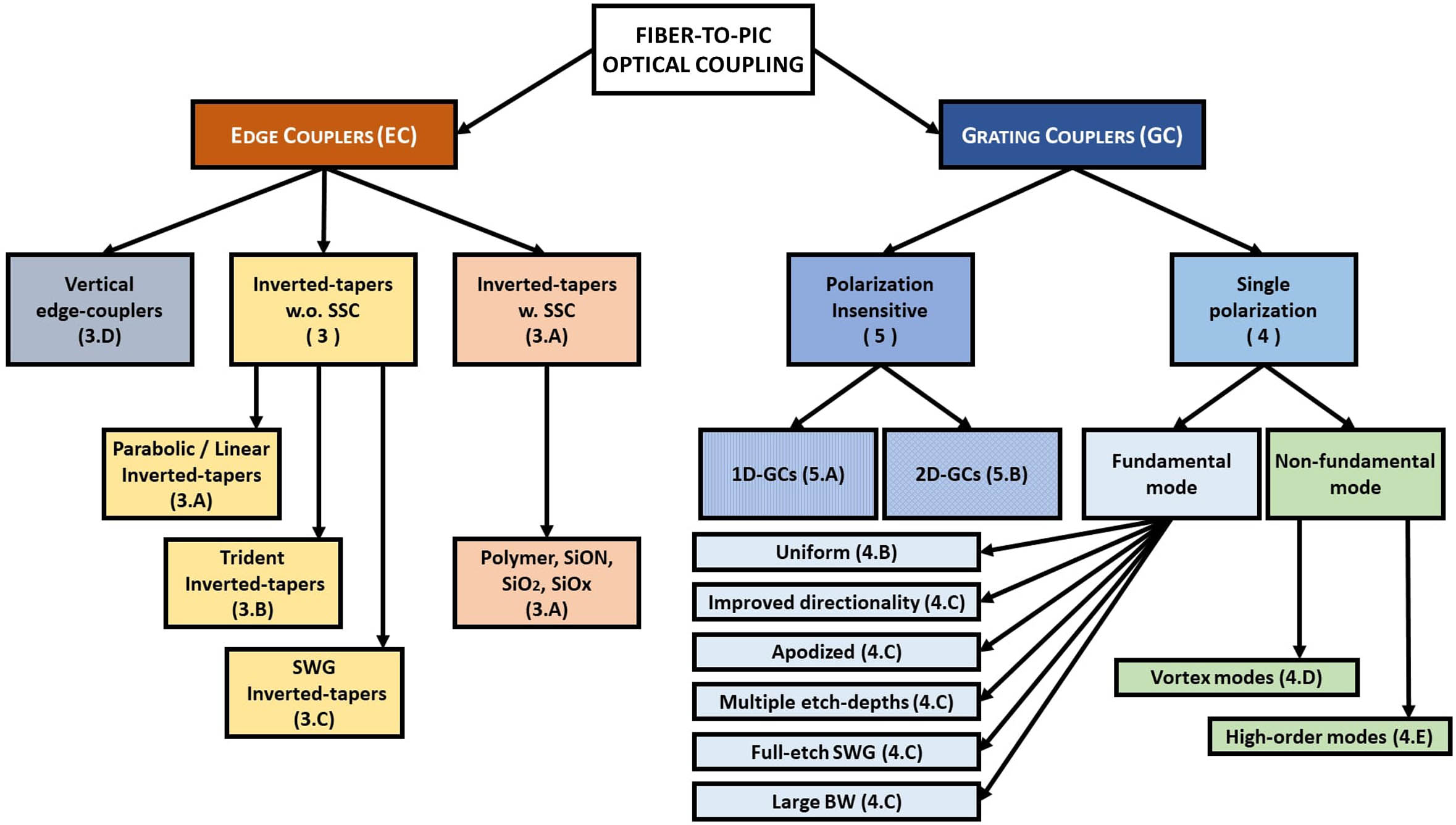
The paper is organized as follows (see Fig. 1). Section 2 gives an overview of the different fiber types commonly used as the interface of photonic integrated circuits. We then focus attention on edge-coupling strategies (Section 3), considering inverted tapers (Sections 3.A and 3.B), metamaterials-based structures (Section 3.C), and vertical coupling to bent waveguides (Section 3.D). Section 4 reports on the principle, design, and optimization of grating coupler (GC) structures for single-polarization beams, considering different materials, fabrication techniques, approaches, and specific applications. We then discuss polarization-insensitive GCs in Section 5, where we analyze 1D and 2D photonic structures (Sections 5.A and 5.B, respectively). Finally, Section 6 is devoted to packaging techniques and reports on the opportunities and limitations connected to the use of fiber arrays, microlenses, and photonic-wire bonds. As a conclusion, in Section 7, we offer a comprehensive table, summarizing in a compact form the main data discussed in the review, which can also be used by the reader as a reference while reading. A schematic representation of the conceptual organization of the topics discussed in the text is given in Fig. 1.
The basic structure of a silicon-on-insulator (SOI) wafer includes the presence of a thick Si substrate, a bottom oxide layer (BOX), a thin Si layer, and eventually of a top oxide layer (TOX). In the following, we will indicate the thickness of the BOX, Si thin layer, and TOX with , , and , respectively.
2. STANDARD AND COUPLING-DEDICATED OPTICAL FIBERS
The interface between a silicon photonics circuit and any optical fiber component typically includes a section of fiber that is either a standard straight-polished fiber or a specialized device that, on some occasions, makes it possible to improve the overall coupler efficiency. In this section, we briefly review the fiber solutions currently being considered by researchers and market specialists.
The standard fiber for telecom and datacom photonic applications is single-mode, generally indicated as single-mode fiber (SMF) 28 [shown in Fig. 2(a)], which shows an attenuation coefficient lower than 0.18 and 0.32 dB/km at wavelengths of 1.55 and 1.31 μm, respectively, and corresponding mode field diameters (MFDs) of 10.4 and 9.2 μm [14]. The SMF28 fiber, whose structure is schematically illustrated in Fig. 2(a), consists of a 125 μm cladding layer ( at ), surrounding an 8.2 μm core, which has a refractive index () that is just 0.3% higher than . Polarization-maintaining fiber variants of SMF28 are available (typically referred to as P-SMF or PMF28), and they use internal stressor rods, in the fiber-cladding region, to induce birefringence so that the mode degeneracy due to the cylindrical symmetry of the fiber core is broken. This slight asymmetry is sufficient to suppress the random polarization hopping, which occurs in standard SMF28 because of external mechanical vibrations or temperature shifts [15]. In general, PMF28 tends to be used in high-value, low-volume applications only because its cost-per-length is one order of magnitude higher than that of standard SMF28, and it also exhibits higher propagation losses than SMF28.
Figure 1.Conceptual organization of the different structures proposed for optical coupling and discussed in the present text.
Figure 2.(a) Cross-section schematic of an SMF28 fiber, showing the 8.2 μm fiber core centered in the cladding layer, wave-guiding the 10.4 μm MFD 1.55 μm mode. Side view schematics of (b) planar polished, (c) angle polished, and (d) lensed SMF28. (e) Schematic of UHNA-to-SMF28 splicing, showing the thermally expanded adiabatic taper. The (b), (d), and (e) geometries are commonly used for edge coupling, while the (c) geometry is preferred for grating coupling.
Visible-light analogues of SMF28 are also commercially available, with reduced MFDs of the order of 4–7 μm, which scales with the typical target wavelength range of 0.60–0.85 μm [16]. There is no single dominant standard for single-mode visible-light fibers because they tend to be used in highly application-specific devices, such as a biosensor, where there is no need for easy integration into a fiber-network. As a result, while SMF28 dominates the telecom and datacom markets, there is a rich ecosystem of visible-light SMFs with different diameters, core sizes, and numerical apertures.
When the SMF28 facet is planar-polished, as shown in Fig. 2(b), the fiber mode diverges into the air with a nearly perfect symmetric Gaussian 2D profile and a numerical aperture of 0.12, which gives a Rayleigh length of the order of 50 μm [17]. Alternatively, the SMF28 facet can be angle-polished (usually to 40°) [see Fig. 2(c)] to facilitate fiber-to-photonic integrated circuit (PIC) grating-coupling. In this geometry, the fiber mode undergoes total internal reflection (TIR) when it is incident on the angled facet and exits the fiber nearly orthogonal to the direction of the fiber core.
The SMF28 facet can also be polished or laser-ablated into a hemispherical (or conical) tip, which acts to focus the 10 μm MFD of the fiber core to a 2–4 μm diameter “hot spot” located 20–40 μm from the end of the fiber, as illustrated in Fig. 2(d). At the focal point, the resulting focused fiber mode offers improved modal overlap with silicon-nitride () spot-size converters (SSCs) generally used in an edge coupler-based silicon-on-insulator (SOI) photonic platform [18]. This approach significantly improves the efficiency of fiber-to-PIC edge coupling, though the smaller spot sizes result in proportionally tighter alignment tolerances. A lensed SMF28 is well suited to single-fiber edge coupling but does not scale efficiently to multifiber coupling (see Section 6) because the mutual alignment of multiple-lensed fibers into an array is practically challenging.
An alternative approach involves using ultrahigh numerical aperture (UHNA) fibers, which use a between the core and cladding refractive indices much higher than that of an SMF28 in order to provide a fiber mode with in the O and C bands [19]. A planar-polished UHNA fiber offers good modal overlap with the SSCs on standard SOI edge couplers and can be spliced to an SMF28 fiber with very low losses () [see Fig. 2(e)], thus guaranteeing easy compatibility with standard fiber networks [20]. Additionally, multiple UHNA fibers can be aligned into a single V-groove array and then planar-polished to create a common facet for the resulting fiber array (FA). This assembly offers improved fabrication tolerances compared with arrays of lensed fibers and is well-suited to multifiber edge coupling of PICs.
3. EDGE COUPLING
This section is dedicated to the analysis of coupling solutions exploiting end-fire coupling schemes. Typically, when one of these schemes is adopted, the incoming and outcoming optical fiber needs to be tailored according to the coupling scheme; therefore, it is crucial to carefully select the proper fiber geometry. For a list of fiber solutions, we refer the reader to Section 2.
A. Inverted Taper-Based Solutions
A basic edge coupler (EC) consists of an inverse taper section, i.e., the waveguide width is gradually reduced along the direction of light propagation, down to a small value at the end tip. As the waveguide dimensions decrease, the guided mode becomes less confined, and its effective cross-section increases, while its effective index decreases. This allows for coupling to a (usually lensed) fiber with a coupling loss determined by effects such as reflection at the chip facet, fiber-to-tip mode mismatch, and mode-conversion loss along the tapered SOI waveguide. Typically, tapers longer than 100 μm are required for adiabatic conversion of the optical mode in the waveguide [21], which is contrary to the drive to minimize the dimensions of photonic components, in order to achieve dense on-chip integration.
In the effort to reduce the EC dimensions, Almeida et al.[22] demonstrated a compact tapered coupler, in which a single-mode SOI waveguide, having a cross-section equal to , was tapered down to a 100 nm wide tip over a length of only 40 μm, using a parabolic-shaped transition. Numerical simulations carried out using a 2D finite-difference time-domain (FDTD) approach predicted a taper-induced loss of only 0.25 dB (assuming a minimum taper length of 40 μm and a minimum tip width of 120 nm). The experimental coupling efficiency (CE) between the taper and a 5 μm MFD fiber was found to be () for transverse magnetic (TM) light polarization and () for transverse electric (TE) polarization, at [22]. The 1-dB bandwidth with respect to fiber misalignment was assessed to be . The reason for the relatively low CE can be explained by the fact that the mode mismatch between the tip and the fiber is minimized for two different values of the tip width, when considering TE and TM polarization, respectively (the optimum tip width value was found to be 50 nm for TM polarization and 120 nm for TE polarization). Also, the guided mode is enlarged only in the in-plane direction, and so a high mode mismatch is still present between the fiber and the tip. To achieve better efficiency, the wave-guided mode must undergo an expansion not only in the in-plane but also in the out-of-plane direction. This can be achieved by fabricating a 3D waveguide taper, where the waveguide height (and not only the width) is gradually varied along the direction of light propagation, as reported in [23,24]. The fabrication processes required for these types of tapers involve gray-scale masks and ultraviolet (UV) gray-scale lithography, which are rather complex and not immediately compatible with the two-tone lithography in standard CMOS process flows.
Another possibility, which is more viable from a mass fabrication perspective, is encapsulating a lateral Si inverse taper structure inside an additional overlay with a lower refractive index material, in order to implement a 2D spot size converter (SSC). This approach is schematically shown in Fig. 3 and allows for subdecibel CEs, for both TE and TM polarized light, over a large spectral bandwidth (1-dB bandwidth ).
Figure 3.Schematic of a standard SOI EC for coupling light between an SOI waveguide and a tapered single-mode fiber. The waveguide (WG) is tapered down to a small tip to allow mode expansion in the horizontal direction, whereas an overlay of polymer, , SiON, or , is deposited over the taper, to allow mode expansion in the vertical direction.
The SSC can be implemented using polymer materials [18,25,26], silicon oxynitride ( or SiON) [27], silicon-rich oxide () [28] or . Considering the SOI platform, the standard SSC is realized in because it can be grown on the Si layer of the SOI wafer using CMOS compatible processes. The refractive index of is approximately 2.0 in the O and C bands, which lies almost exactly between the effective index of an SMF28 fiber and the waveguides on the SOI platform, allowing for nearly optimum index-matching conditions. A standard SSC has a cross-section on the order of . Growing thicker layers of , to implement SSCs for beams exhibiting a larger MFD, is quite challenging because the stress added to the SOI wafer during the growth process could lead to wafer-bowing and even fracturing. An increase in the MFD of an SOI EC, to better match the 10 μm MFD of SMF28, can be achieved by using a silicon oxynitride SSC. By properly tuning the ratio between and gases used during the SSC-layer deposition, a continuous variation of refractive index from 2.0 (pure ) to 1.5 (pure ) can be achieved. The resulting graded-index SiON SSC can provide an MFD of 6–10 μm, which offers good modal overlap to planar-polished SMF28 as well as improved index-matching. These recent developments have been well received by the photonic foundries, allowing them to relax fiber-to-PIC alignment tolerances and reducing the need for expensive, specialized fibers, such as lensed SMF28 and UHNA fibers.
To provide close access to optical waveguides and ECs, the edges of the PIC die are typically polished to achieve optical-quality facets. Although this process is well established and works well at small volumes, its scale up to large volumes is not practical. Therefore, other solutions for creating optical facets on PICs are being investigated. For instance, the optical facet can be realized using a two-step reactive ion-etch (RIE) process [29], where (i) a first etching step is used to fabricate high optical quality trenches through the SSCs and into the first few μm of the SOI surface and (ii) a coarser deep-etching step is used to create an approximately 80–100 μm deep trench into the SOI substrate to facilitate fiber access and positioning, as shown in Fig. 4.
Figure 4.(a) SEM image of the optical facet and edge-coupler region on an SOI-PIC, showing the mirror-finish optical facet, deeper RIE trench for fiber access, and the diced edge of the PIC for singulation from the rest of the wafer. (b) Schematic of a multichannel fiber array, showing the 250 μm pitched array of fibers sandwiched between a V-groove array and a contact plate.
For example, in [18], an inverse taper was designed to reduce the width of a Si wire waveguide down to 60 nm over a 200 μm length. Both the waveguide and the taper were fabricated by e-beam lithography and electron cyclotron resonance (ECR) plasma ion etching and then encapsulated in a polymer waveguide. Experimental measurements showed a CE of 83.2% () and a polarization-dependent loss (PDL, defined as the CE variation when changing the polarization of the input fiber optical signal from TE to TM) of about 0.5 dB, for an optical fiber with an MFD of 4.3 μm.
A similar inverse taper structure was demonstrated in [27], regarding Si wire waveguides and SiON-SSCs, deposited by means of plasma-enhanced chemical vapor deposition (PECVD). The use of SiON allowed for better durability and resistance to humidity (with respect to polymer materials) as well as lower absorption in the telecom C band. This approach resulted in a measured CE of 89.1% () (for a 4.3 μm fiber MFD) and a 350 nm increase in bandwidth, with respect to [18], due to reduced absorption by the CH bond in the SiON material. Measurements carried out using larger MFD fibers (9 μm) showed a maximum CE of 56.2% ().
Another high-efficiency SOI EC (optimized for TE light polarization) was demonstrated by McNab et al.[26], with a Si wire waveguide having a cross-section. The authors took into consideration the polymer SSC inverse taper structure reported in [18] and optimized it in order to improve the CE for TE light polarization at the expense of the PDL. This approach allowed shortening the taper down to 150 μm, with respect to 200 μm, as used in [18], by realizing a polymer waveguide with a cross-section of , while increasing the tip width to 75 nm (thus relaxing the fabrication tolerances). As a consequence, the improved design allowed for a measured CE for TE polarization of 89.1% () at , with a nearly flat spectral response over a 300 nm bandwidth. The CE for TM polarization was instead found to be about 79.4% (). The tolerance to lensed fiber misalignments was also experimentally characterized, recording a 3 dB efficiency drop for a 1 μm displacement from the optimal position, thus proving how critical the fiber alignment is for achieving high coupling efficiency with edge couplers. All of the inverse tapers reported in [18,26,27] were fabricated with e-beam lithography, in order to realize sufficiently small tip widths. In contrast, the work described in [25], used an inverse taper with a 175 nm tip width [thus compatible with 248 nm deep UV (DUV) lithography], which was designed for a Si wire waveguide having a cross-section. It was theoretically shown that a CE of about 87.1% () could be achieved, without excessively increasing the taper length, by placing a benzocyclobutene (BCB) spacing layer (with thickness of 200 nm) between the taper and the polymer waveguide and by reducing the polymer waveguide height from 3 μm (the value reported in [18]) to 1.3 μm. The experimental characterization carried out over fabricated samples with optimum design reported, however, a fiber-taper CE of only 64.6% ().
In [28] instead, a Si strip waveguide with a thickness of 220 nm (S) and initial width of 500 nm, was linearly tapered down to 80 nm over a length of 300 μm, by means of 193 nm DUV lithography and RIE techniques and then encapsulated in a SSC ridge waveguide. This allowed experimental demonstration of CE as high as 94.4% () at a wavelength of 1.55 μm for both TE and TM polarizations, by using a lensed fiber with for coupling.
A number of different types of SOI ECs were reported in the scientific literature, such as those employing multilevel Si inverse tapers [30,31] or using a waveguide as an SSC [31,32]. In [30], for example, it was theoretically shown that the CE between a lensed fiber and a 500 nm high Si wire waveguide could be increased up to 90% () by using a double-layer inverse taper, in which the top layer is composed by a parabolic tapered section, followed by a sine tapered section. Two overlapped Si tapers were also employed in [31], with the double taper located inside a suspended waveguide (), used for mode size conversion (see Fig. 5).
Figure 5.Schematic of the SOI edge-coupling structure proposed in [31], based on the use of a double-layer Si inverse taper and a waveguide. Reproduced from [31].
The device was fabricated starting from an SOI wafer with and ; in addition, 248 nm DUV lithography was used to pattern both the wire waveguides () and the tapers (both taper layers have a 110 nm wide tip), which were then defined by two different etching processes, one partial 140 nm deep etch and a full etch. The encapsulating waveguide was then obtained by growing a 4 μm thick layer (by means of PECVD) over the BOX and by using an octofluorocyclobutane () and sulfur fluoride () based etch to define the suspended structure, which is essential to prevent light dispersion in the BOX and in the Si substrate. The experimental CE for the fabricated device, when using a lensed fiber with 5 μm MFD, was between 67.6% () and 63.1% () for TE polarization and between 63.1% () and 57.5% () for TM polarization, in the wavelength range of 1.52–1.60 μm. The alignment tolerance was also characterized, with a 1 dB efficiency drop for a 1.7 μm displacement from the optimal coupling position. When coupling light from a cleaved fiber with 9.2 μm MFD, the CE was reduced to 39.8% () for both TE and TM polarizations, but with 1 dB misalignment tolerance increased to . In [32], a Si inverse taper was designed in an SOI platform with and , exploiting the thicker BOX to implement a waveguide underneath the taper, which acts as a SSC. The Si wire waveguide () was tapered to a 200 nm width over a length of 400 μm, whereas the cross-section of the waveguide was set to ; the Si substrate was also etched in order to create a V-groove structure for allowing fiber passive auto-alignment techniques (see Fig. 6). When considering a fiber MFD of 8 μm, CEs of 44.7% () and 42.7% () were theoretically demonstrated for the TE and TM polarizations, respectively, at .
Figure 6.Schematic of the SOI edge-coupling structure proposed in [32], based on the use of a Si inverse taper and a waveguide implemented in the BOX. A V-groove is etched in the Si substrate to allow for fiber auto-alignment. Reproduced from [32].
Recently, Hatori et al.[33] proposed an alternative method to design silicon photonic inverted tapers, without the need for 3D structures or overlay waveguides. The authors’ coupler is composed of a three-waveguide structure, implemented in an SOI platform () and having an overall length of 150 μm, as shown in Fig. 7. The topology includes a main tapered Si wire waveguide in the center, and two secondary tapered waveguides placed symmetrically to the sides of the main taper.
Figure 7.(top) Schematic of the SOI trident EC structure proposed in [33]. Reproduced from [34]. (bottom) Top view of the trident SOI EC structure proposed in [33].
The trident design allows greater flexibility during the design phase. In fact, while in standard tapers the mode size at the chip facet is only determined by the tip width (such as in [22]), the resulting mode size from the trident design can be tuned by adjusting the distance between the two lateral waveguides and the width of their tips. In order to obtain a 3 μm guided mode spot size at the chip facet, the distances between the secondary waveguides and the width of their taper tips were set to 1 μm and 150 nm, respectively. This acts to prevent the excitation of high-order guided modes. The width of the side waveguides was set to 300 nm, while the widths of both the lateral ending tip and central waveguide tip, were set as 100 nm: these values allowed the modal mismatch between the two discontinuities inside the coupler to be minimized. Test structures with a different number of trident elements were designed and fabricated, to experimentally assess the fiber-waveguide CE and the excess loss. At the central wavelength of , the CE for TE and TM input polarization was equal to 80.9% () and 80.5% (), respectively. The simulated CE values were 92.5% () and 86.7% (), respectively, giving an excess loss of 0.55 and 0.24 dB, respectively.
C. Metamaterial-Based Edge Couplers
An alternative solution to implement highly efficient planar ECs, without the need of an overlay SSC, relies on the use of subwavelength gratings (SWGs) [35–37]. As shown in Fig. 8, an SWG consists of a Si wire waveguide in which fully etched trenches are periodically formed along the direction of light propagation. If the period of the grating is smaller than the optical wavelength and is also small enough to avoid Bragg diffraction, then the SWG can be treated as a metamaterial, according to effective medium theory [38]. The effective refractive index of this structure can be varied between that of Si and of the cladding material, by changing the grating duty cycle, i.e., the ratio between the length of the unetched grating portion and the grating period .
Figure 8.SEM image of an SWG waveguide. Inset shows the dispersion diagrams (for TE polarization) of an SWG waveguide (blue curve) and of a standard strip waveguide (red curve) having an effective refractive index of 2.65. The two curves show a good match when away from the bandgap resonance. Reproduced from [36].
Implementing a Si inverse-taper-based EC with the aid of an SWG structure offers a fundamental advantage with respect to standard Si inverse tapers. Narrow waveguide tips are often required for high-efficiency taper-based EC designs, and these require e-beam fabrication. Additionally, given that the optimal tip size for TE and TM polarization is generally different, these designs result in couplers with high PDL [22]. In contrast, SWG-based structures offer an extra degree of freedom that is useful at the design stage because the spot size at the coupler tip can be controlled by both the tip width and the waveguide effective refractive index, which can be tuned by modifying the SWG structure.
Cheben et al.[35] carried out the first analytical study of SWG-based ECs for coupling light into an SOI strip waveguide. The authors focused on an SOI platform with and a cladding (). An SWG structure with a constant period was implemented, with a duty cycle linearly chirped from 0.1 (at the tip of the coupler) to 1 (at the conjunction with the strip waveguide), in order to allow the SWG effective refractive index to evolve along the direction of light propagation. Different coupler lengths (from 10 to 60 μm) and profiles, including lateral tapering (by one- or two-step linear width tapering) and vertical tapering (by RIE lag effect), were analyzed. The performance of the different SWG-based EC configurations was evaluated by means of 2D-FDTD numerical simulations.
The best results were obtained when numerically simulating an SWG coupler with a length of 50 μm and two-step linear width tapering, where the SWG width was initially varied from 30 nm (at the tip of the SWG) to 150 nm along the first two-thirds of the coupler length and then from 150 to 300 nm, without any tapering of the SWG height. This configuration showed a theoretical CE of 76.1% () at , when coupling light from a standard SMF having an MFD of 10.4 μm and a CE of 81.4% () when using a high numerical aperature (NA) fiber with a reduced MFD of 5.9 μm (see Section 2). Despite the good coupling performance, it should be noted that no fabrication-related constraints were considered during the theoretical optimization. As a result, the optimal tip width is 30 nm, which is far below the resolution of the lithographic process currently employed by silicon photonics foundries.
The first experimental demonstration of such an SWG-based EC was reported by the same research group in [36], using an SOI platform, with , , and a 2 μm thick SU-8 () polymer layer as the top-coating material. The SWG period was chirped from 400 nm (at the coupler edge) to 200 nm (at the junction with the strip waveguide) while simultaneously tapering the width from 350 to 450 nm, so as to match the width of the strip WG. The taper itself was composed of two different sections: in the first low-confinement section, close to the chip-edge, the grating gaps were fully etched, with their length linearly decreasing from 200 to 170 nm, whereas, in the second section, the gaps had a constant length of 100 nm and were partially filled by Si bridging elements, having a width linearly increasing from 100 to 450 nm, so as to obtain a smooth transition from the SWG to the strip waveguide. The average values of the experimentally measured CE, at and using a lensed SMF with 2 μm waist, were assessed to be 81.3% () and 75.9% () for TE and TM light polarization, respectively. As the SWG is based on a nonresonant phenomenon, the transmission band was found to be almost flat for more than 100 nm. The system also showed good tolerance to fabrication-induced feature-size variations, as a change of tip width from 350 to 300 nm led to an increase of the insertion loss by less than 0.1 dB for both polarizations.
Starting from the SWG-based EC configuration described in [36], a refined design was proposed in [37], which showed improved performances in terms of CE and PDL. A schematic representation and a scanning electron microscope (SEM) image of the improved SWG edge coupler are shown in Fig. 9.
Figure 9.(a) Schematic representation of the SWG-based EC described in [37]. (b) SEM image of the fabricated SWG-based EC. Reproduced from [37].
This coupler was implemented in a standard SOI platform (, ) using as cladding material. Comparing this structure with the one previously reported, the thicker BOX (3000 nm instead of 2000 nm) allowed for reduction in parasitic coupling to the substrate, thus improving the overall performance. As shown in Fig. 9, the coupler is still composed of two different sections, similar to the one reported in [36]. The design consists of an initial low-confinement section with fully etched gaps, followed by a second transition section with the gaps partially filled with Si bridging elements. The initial section was designed to have a tip width of 220 nm, and both the grating period and duty cycle were engineered to obtain an optical MFD at the chip edge equal to 3.2 μm. The use of a square-shaped tip allows the PDL to be essentially eliminated (the residual PDL is 0.01 dB); this is ultimately limited by the residual vertical asymmetry of the structure, due to the presence of a Si substrate under the BOX, while air is present above the cladding. It is important to note that it is not currently easy to realize polarization-insensitive inverse tapers using a standard SOI configuration. This is due to the fact that the optimal tip width for TE and TM polarization is lower than the standard Si layer thickness of commercially available SOI wafers [22]; thus, solutions to reduce the Si layer height should be included in the process [4].
Another aspect that was improved with respect to the initial design in [36] was the transition between the first and the second section of the SWG coupler, where an effective index mismatch at the junction led to an extra loss of 0.3 dB. This loss originated from the difference between the volume fraction of silicon (the high index material of the grating) at the junction between the fully etched and partially etched sections [see grating elements labeled A and B in Fig. 9(a)]. In order to mitigate this issue, thus reducing the excess loss, the width of the first element (A) of the fully etched section was slightly increased with respect to the corresponding element in the partially filled section (B), approximately by the size of the first Si bridging element (C). Some test structures of the nominally optimized design were fabricated using e-beam lithography to pattern the SWG and showed an experimental CE of 89.1% () with an extremely low PDL (). Even better CEs were obtained by two additional designs with a small bias on the tip width ( or ): the first one resulted in a CE of 91.2% () with negligible PDL, whereas the second one resulted in a CE of 92.9% () (for TE polarization) with a PDL of 0.5 dB.
Many of the previously discussed edge coupling solutions made it possible to to obtain CEs better than , although they required the use of relatively expensive tapered or lensed fibers for mode-matching. In contrast, Papes et al.[39] recently theoretically demonstrated the possibility of achieving efficient edge coupling using standard cleaved SMF-28 fibers with a 10.4 μm MFD, or high numerical aperture (HNA) fibers with a 6 μm MFD, which represent a good trade-off between tapered/lensed fibers and standard SMF-28 fibers. This was facilitated by the use of a standard linear Si taper (with a tip width of 150 nm), in a 220 nm Si thick platform having a 3 μm BOX layer and with an increased upper cladding refractive index near the chip facet, achieved via the deposition of a stack of layers, as shown in Fig. 10.
Figure 10.Schematic representation of the EC structure optimized for a 10.4 μm MFD, presented in [39]. A ridge waveguide is formed in the upper cladding over the Si inverse taper, and layers are deposited in order to increase the effective refractive index of the upper cladding. The dimensions are not to scale.
This technique allowed the optical mode dimensions at the chip edge to be increased, while simultaneously pulling it toward the upper cladding and therefore helped to reduce optical leakage to the Si substrate, as shown in Fig. 11 (bottom). At the same time, the layers (20 nm thick and 30 nm thick, respectively, for the 6 μm MFD and the 10.4 μm MFD fibers) were patterned as SWGs with varying duty cycle to gradually reduce the effective refractive index of the layers from that of pure () in correspondence with the coupler tip, to that of pure () at the end of the layers.
Figure 11.Fundamental TE mode distribution at the coupler tip, of the structure optimized for a 10.4 μm MFD. The mode is pulled toward the upper cladding, therefore overcoming optical leakage to the Si substrate. Reproduced from [39].
The performances of the different edge coupler configurations were numerically evaluated using a mixed 3D-FDTD and 3D eigenmode expansion (EME) approach for the 6 μm MFD configuration and a pure 3D-EME approach for the 10.4 μm MFD configuration, resulting in a CE of 90.8% () and 84.1% (), respectively, at for TE mode. The wavelength dependence of the coupling efficiency for both configurations was evaluated by means of 3D-EME simulations, showing variations of less than 0.2 dB over the 1.45–1.60 μm wavelength window. The 1 dB fiber misalignment tolerance was also assessed to be 1.3 μm for a 6 μm MFD and 2.2 μm for a 10.4 μm MFD, which is larger than that reported for standard inverse-taper ECs.
D. Vertical End-Fire Couplers
One of the main limitations for edge coupling solutions is related to their incompatibility with wafer-level testing of the photonic circuits and devices. A possible solution to this problem has been provided by Yoshida et al.[40–43] who proposed a novel vertical end-fire coupler scheme, also known as an “elephant” coupler. This coupler used a vertically swept SOI strip waveguide, realized by means of an ion implantation process to achieve a radius of curvature in the order of a few μm. An SEM image of a vertically curved coupler is shown in Fig. 12.
Figure 12.SEM image of a vertically bent optical coupler, obtained by ion implantation in a silicon waveguide. The bent waveguide is 5 μm long, and the curvature radius is approximately equal to 3 μm. Reproduced from [43].
The vertical couplers described in [41] were implemented in a standard SOI platform having and . The first fabrication step involved the realization of Si wire waveguides with a width of 430 nm and nano-tapers having a 20 μm length and 190 nm tip width, which marks the end of the waveguides. As a second step, the underneath the Si taper was partially removed by wet etching, in order to obtain cantilever structures of different lengths (ranging from 5 to 40 μm). A 0.7 μm thick protective layer was then deposited, to protect the waveguide region outside of the cantilevers, and Si ions were implanted perpendicularly to the chip surface. Si ion implantation (with a penetration depth controlled by the acceleration energy, 80 keV in [41]) increases the concentration of lattice defects near the top surface of the cantilever and produces a spatially confined amorphization of the crystalline silicon. The change of the material structure affects the internal stress of the cantilever, allowing for the engineering of the cantilever bending. As a final step, the bent Si cantilevers were encapsulated in a 2 μm thick cladding, deposited by means of PECVD at 350°C. The longest couplers (having length between 10 and 40 μm) were further reinforced with a spin-cast epoxy resin having a refractive index equal to that of . The optimal ion dose required to obtain a 90° bend varied according to the cantilever length (from for the 40 μm long cantilevers, up to for the 5 μm long cantilevers), as higher internal stress is required to achieve shorter radii of curvature. The main drawback of this technique is due to the additional waveguide propagation loss introduced by the increased concentration of lattice defects. The propagation loss increases from 0.05 dB/μm at to 0.1 dB/μm at , showing saturation for higher levels of ions doses [42].
It is worth noting that the overall coupling loss of the fabricated elephant couplers (including the scattering/absorption loss due to ion implantation, the radiation loss due to bending, and the tip-fiber coupling loss) decreases when relatively short cantilevers are considered. This suggests that a trade-off exists between relatively long (low implantation doses, long propagation distances) and relatively short tapers (high implantation doses, short propagation distances). The measured CE at for 5 μm long vertical couplers, when coupling to a 2 μm spot tip-lensed single-mode fiber, was found to be 60.3% () for TE polarization and 43.7% () for TM polarization, with very low wavelength dependence. It was also shown that this CE could be further improved by performing a 600°C annealing process after coating the cantilevers with . This process makes it possible to recrystallize the previously amorphized silicon, theoretically making it possible to reduce the ion implantation by more than one order of magnitude, without deforming the bended coupler. However, such an annealing process would compromise the fabrication CMOS compatibility, as other devices would be permanently damaged by the high annealing temperatures.
Recently, the same authors also demonstrated the possibility to obtain light coupling between silicon vertical couplers and high numerical aperture fibers (5 μm MFD) [44,45]. Unlike their previous works, this time the Si nano-tapers were designed to show an exponential tapering profile, with the waveguide width decreasing from 430 to 50 nm over a 6 μm length, while the 90° waveguide bending was obtained by means of argon ion () implantation (). A 2.7 μm thick cladding was then deposited over the curved Si nano-taper by means of tetraethyl orthosilicate (TEOS) PECVD: as a result of the isotropic nature of the deposition process, a dome-like structure with 5.4 μm diameter was formed at the coupler cap. This structure basically acted as a collimation lens, making it possible to reduce the high divergence angle of the beam emitted from the Si taper tip (where the high divergence is due to the extremely short taper length), so as to obtain a 5 μm MFD output beam with a nearly flat phase plane. This structure showed a theoretical CE of 83.2% () with a 0.5 dB loss bandwidth of 420 nm for TE polarization, whereas measurements carried out on experimental samples reported a CE of only 38% () with a reduced 0.5 dB loss bandwidth of about 150 nm; the discrepancy between the simulated and the experimental efficiency values can be explained by a reduced radius of curvature of the curved waveguides in the fabricated devices with respect to the nominal value [45].
4. SINGLE-POLARIZATION GRATING COUPLERS
One of the most popular solutions to implement fiber-to-waveguide optical couplers is represented by vertically coupled diffractive grating structures. The wide adoption of these devices in the field of silicon photonics is due to several factors: (i) they provide access to any point on the PIC, thus facilitating wafer-level testing; (ii) they do not require intensive post-fabrication processing, such as cleaving and facet-polishing; and (iii) they typically provide relatively relaxed fiber-positioning tolerances, usually higher than that of typical ECs (see Section 3). A diffractive GC is realized by varying the waveguide refractive index profile according to a periodic pattern defined along one or more dimensions. This allows for phase-matching between the (near vertical) optical mode incident on the grating structure and the Si waveguides in the horizontal plane of the PIC (see Fig. 13).
Figure 13.Schematic representation of a 1D-GC used as an outcoupling device. Si layer thickness, BOX layer, etched depth, and fiber core are shown with the right relative proportions.
If the refractive index distribution is engineered only along the direction of light propagation, then a 1D-GC is obtained. If the refractive index is also varied along the width of the waveguide, then a 2D-GC is realized. SOI-based integrated waveguides usually exhibit a high birefringence, thus making it challenging to achieve efficient coupling into a standard 1D-GC for both the orthogonal (and degenerate) light polarization states propagating in an SMF. As a consequence, 1D-GCs are usually optimized for a single state of polarization, whereas more complex structures are required to implement polarization-insensitive couplers. This section is focused on single-polarization 1D-GCs. We first describe the working principle (in Section 4.A); subsequently, we review some of the most relevant 1D-GC structures proposed in the scientific literature (Sections 4.B and 4.C); then, we will also report about GCs suitable for vortex modes and higher-order modes (Sections 4.D and 4.E). Polarization-insensitive GCs instead are discussed in Section 5.
A. Introduction to 1D Grating Couplers
1. Structure and Working Principle
In a GC structure, the refractive index variation can either be periodic (uniform GC) or nonperiodic. Nonperiodic grating structures are usually referred to as “apodized” or “chirped” gratings. Here, we will take into account a uniform 1D-GC implemented in a standard SOI platform, as shown in Fig. 14, where the vector of the waveguide mode and the waveguide effective index variation are assumed to develop along the axis.
Figure 14.Cross-sectional schematic of a uniform GC implemented in SOI technology.
The periodic index variation is created by partially etching the Si waveguide with an etch depth , thus defining etched trenches with length and original thickness (i.e., unetched) teeth with length . The period is defined as the length of each scattering unit, thus being The grating fill factor (FF) can be defined as the ratio between the unetched tooth and the grating period [see Eq. (2)], even if some authors [46] define the fill factor FF as the ratio between and : As a first-order approximation, the effective refractive index () of the waveguide grating section can be defined as a function of the effective index of the unetched tooth and of the etched trench (labeled as and , respectively), as shown in Eq. (3). The resulting of the grating is therefore influenced both by the choice of the FF and by the chosen value of , as increasing the etch depth causes a reduction of : The grating structure can be exposed to air (as shown in Fig. 14), or it can be coated with a top oxide layer.
In the following, we describe the basic working principle of a 1D-GC. For the sake of simplicity, we consider its use as an outcoupling device (i.e., used to couple light from the integrated chip to an optical fiber), but an analogous description holds when the grating is used as an incoupling element.
The physical behavior of a diffractive GC can be described in terms of the Bragg condition, which defines the relation between the wave vector of the incident optical beam and the wave vectors of the diffracted beams. With reference to Fig. 14 (where the index variation is introduced along the axis), the Bragg equation can be expressed as where is the diffraction order, is the axis component of the wave vector of the th diffracted order , is the propagation constant of the waveguide guided mode, and is a vector lying in the direction, which describes the grating according to the following expression: If we take as the refractive index of the top medium and as the refractive index of the bottom medium (which is the BOX in this case), the wave vector of the th diffracted order can be expressed according to Eqs. (6) and (7), whereas the waveguide propagation constant can be expressed according to Eq. (8), being the effective refractive index of the waveguide grating [see Eq. (3)]: The Bragg condition [Eq. (4)] describes phase-matching along the axis for the modes diffracted by the grating.
A pictorial representation of the Bragg condition, expressed by Eq. (4), can be obtained by means of wave-vector diagrams (e.g., Fig. 15). Ideally, the grating is located in the center of the diagram, and concentric semicircles are drawn around it, with a radius directly proportional to the magnitude of the optical wave vector k in the corresponding medium. Using these types of diagrams, the th order diffracted beam can be graphically constructed by adding times the grating vector K to the axis component of the wave-guided beam (blue vector) and then by tracing vertical lines from the end point of the resulting vector, perpendicularly to the interface of the two circles. If the vertical line crosses the wave-vector circle, then the th order diffracted beam is permitted, with its vector starting at the center of the circles and ending at the intersection point. Conversely, if there is no intersection between the semicircle and the vertical line, then the diffracted mode has no physical meaning. Two scenarios are of particular interest: in Fig. 15 we show the situation occurring when (i.e., the optical wavelength inside the grating). In this configuration the 1st order diffracted mode is vertically emitted from the grating and can therefore be coupled to an optical fiber, but the 2nd order diffracted mode is reflected back to the waveguide. This configuration, also known as resonant configuration, is usually not employed in practice, unless a specific strategy to suppress the reflected contribution is adopted. This can be realized, for example, by implementing a partially reflecting mirror before the grating, as reported in [47]. On the other hand, if we consider the case (see Fig. 16), the 1st order diffracted mode is emitted with its direction slightly detuned from the vertical axis, while the 2nd order in-waveguide reflection contribution is suppressed. Given the considerable advantages of this setting, this configuration is the most widely adopted in designing 1D-GCs. By considering the 1st order diffraction angle () in the detuned configuration, the Bragg condition of Eq. (4) can be reformulated as This equation shows that, when an optical beam having a central wavelength interacts with a uniform GC, it is diffracted at an angle , which can be tailored by appropriately adjusting its geometrical parameters (, , FF). Both in the resonant and in the detuned configurations, two 1st order diffracted contributions exist: one is emitted upward (i.e., toward the collection fiber), while the second one downward toward the substrate. This practically implies that part of the optical power incident on the grating will be directed toward the substrate, representing a power loss. It is also important to note that the Bragg condition is strictly valid only for infinite grating structures and for small index variations. For a finite structure, diffraction does not occur at a single discrete -vector only but for a range of -vectors around that predicted by the Bragg condition. As a result, real GCs show a nonzero spectral bandwidth for waveguide-to-fiber coupling.
Figure 15.Wave-vector diagrams of waveguide GCs in resonant configuration.
SOI-based GCs can be implemented by etching vertical trenches in the Si slab, resulting in square-shaped devices, as shown in Fig. 17(a). In this case, the width of the grating (along the direction, with reference to Fig. 17) is usually chosen to be about 12 μm [48], in order to properly accommodate the Gaussian beam emitted by an SMF fiber typically exhibiting a 10.4 μm MFD. In this case, a linear taper whose length is in the order of hundreds of μm (400 μm, for example, in [48]) is required to connect the wide grating section to the submicrometer-sized Si waveguide, thus allowing for low-loss mode conversion. An alternative solution is to use a focusing configuration [49], as shown in Fig. 17(b), which allows one to considerably reduce the coupler footprint space. In this case, the grating trenches are no longer straight lines but describe sections of different ellipses, all having a common focal point located between the integrated waveguide and the coupler section. If the grating surface lies in a plane of coordinates and (according to Fig. 17), where is the direction of light propagation and the origin is set in the desired focal point, the focusing grating can be defined by curving the grating trenches [50], so that where is an integer number for each grating trench, is the angle between the fiber and the chip surface, is the external refractive index, is the optical wavelength in vacuum, and is the effective refractive index experienced by the cylindrical wave in the grating section. If a straight-trench grating and a focusing grating are characterized by the same etch depth, period, and fill factor, their CEs are almost exactly the same; when designing a focusing grating, it is therefore convenient to initially assume a straight-trench configuration and, once the optimal geometrical parameters (period, fill-factor, etch depth) have been identified, use them to curve the grating according to Eq. (10).
Figure 17.(a) Schematic top view of a GC with straight trenches. (b) Schematic top view of a focusing GC.
The performance of a generic GC is typically determined by three parameters.
Directionality: the ratio between the optical power diffracted upward () toward the fiber and the optical power propagating along the integrated waveguide before the grating (). ( and are defined with reference to Fig. 14.)
Reflectivity: the ratio between the optical power reflected back to the waveguide by the GC and the optical power impinging from the waveguide on the GC (). A nonzero reflectivity is always present, even in detuned grating configurations, because of the refractive index contrast between the Si waveguide and the grating section; it is important to minimize this effect, as it can cause parasitic Fabry–Perot oscillations in the PIC.
Overall coupling efficiency: the ratio between the optical power coupled to the fundamental mode of the optical fiber and the optical power propagating along the waveguide (). Thanks to the reciprocity theorem, which can be applied to linear open systems as silicon gratings, if we consider single-mode waveguides and single-mode fibers, the CE in the output configuration (i.e., light travels from the PIC waveguide to the fiber) and in the input configuration (i.e., light couples from the fiber to the PIC waveguide) is exactly the same [51].
In order to provide the reader with reference values, which are useful to better understand the advantages and disadvantages of structures proposed in Sections 4.B and 4.C, we describe in the following the typical performance offered by a 1D-GC with standard design and fabrication parameters.
2. Performance of Uniform Grating Couplers
For a uniform GC (UGC) based on a standard SOI platform, having and , the maximum CE is usually achieved for shallow etching levels () and FF values close to 0.5, and it is limited to values . This can be seen in Fig. 18, where the CE spectrum calculated as a function of the wavelength is reported for different values of and FF, assuming TE light polarization (along the direction, with reference to Fig. 14). In these simulations, the grating period was set to 634 nm, so as to obtain a diffraction angle equal to 14.5° for a central wavelength of 1.55 μm. As previously mentioned, a 1D-GC optimized for TE light polarization will suppress light in the opposite polarization, as shown in Fig. 19.
Figure 18.(Top) CE for a UGC implemented in a standard SOI platform ( and ), with a grating period and . CE is reported as a function of optical wavelength for different values of etching depth , ranging from 60 to 80 nm. (Bottom) CE for a UGC implemented in a standard SOI platform ( and ), with a grating period and . CE is reported as a function of optical wavelength for different values of FF, ranging from 0.4 to 0.6.
Figure 19.CE of a TE-optimized 1D-GC as a function of optical wavelength for TE light polarization (blue trace) and for TM light polarization (red trace).
The low CE of standard UGCs can be explained in terms of poor directionality and poor mode-matching between the radiated field distribution and the Gaussian field distribution of the fundamental mode of an SMF.
Concerning directionality, a considerable part of the optical power incident on the GC can be diffracted downward, toward the substrate, unless a proper structure is designed. In a perfectly symmetrical situation, assuming infinitely extending BOX and TOX and full etching of the Si layer, the 1st order upward and downward diffracted modes would have the same intensity, thus clipping the maximum achievable CE to 50%. In practical SOI implementations, part of the power diffracted downward is reflected at the interface between the BOX and the Si substrate, thus making it possible to increase directionality and, consequently, the maximum achievable CE. The GC directionality shows a sine-type dependence on the BOX layer thickness: the maximum directionality values are achieved when the reflected contribution is in phase with the upward diffracted field. However, it is important to note that this parameter generally cannot be optimized in the grating design stage, i.e., it directly depends on the structure of the SOI wafer chosen for fabrication, and other components may define the required BOX thickness. Nevertheless, it is interesting to note that SOI wafers with different geometrical specifications are currently commercially available [52]. Some of the techniques, which have been proposed and demonstrated in the scientific literature to control and boost the GC directionality, will be described in Section 4.C.1.
In order to better understand the mode-matching issue, it is useful to analyze the normalized power density profile radiated from a UGC, as shown in Fig. 20. The specific data refer to a uniform 1D-GC realized in an SOI wafer with and , but similar results are obtained even varying these parameters; thus, the conclusions that can be derived have general validity. As shown in Fig. 20, in UGCs most of the optical power is radiated in the initial section of the grating and then an exponentially decaying trend is observed, which can be expressed as In the above equation, is the grating coupling strength ( for the example of Fig. 20), whose value varies as a function of and FF, as shown, for example, in Fig. 21, where the normalized power density profiles of the diffracted mode are reported, for GC realized in SOI wafers with , having and FF ranging from 0.5 to 0.8.
Figure 20.Normalized power density profile of the diffracted mode from a UGC, implemented in a 220 nm Si thick SOI platform with a 70 nm deep etch.
Figure 21.Normalized power density profile of the diffracted mode from UGCs, implemented in 220 nm Si thick SOI platform with a 70 nm etch depth and FF ranging from 0.5 to 0.8.
Starting from the coupling strength , the grating coupling length (the length of the region inside the grating where spatial transients develop) can be defined as As the fundamental mode of SMF is characterized by a Gaussian distribution, with an MFD of 10.4 μm, the grating-fiber mode overlapping is, however, quite poor (usually ), thus affecting the resulting CE.
B. Grating Couplers for Large-MFD Optical Beams
In this section and in the next, we review the most relevant GC structures present in the literature to date. We start our discussion from the oldest Si-GCs, designed to work at using external collimating optics to in/outcouple light to/from the device. GCs specifically designed for fiber coupling will be extensively discussed in the next section.
The first generation of SOI GCs was developed between the end of the 1990s and the early 2000s. Twenty years after the seminal work published by Neviere [53], Pascal et al. carried out the first analytical study of the interaction of an SOI waveguide grating with an incident Gaussian beam, under the paraxial approximation hypothesis [54]. In this work, the authors found that, in order to maximize the grating CE, the waist of the input Gaussian beam, which was focused on the grating using a discrete-elements optical system to adjust the waist radius, had to be equal to . The theoretical results were confirmed by the experimental characterization of a UGC fabricated using a SIMOX SOI platform ( and ), designed for and showing a maximum CE of about 30% () for an input waist radius of 300 μm. A few years later, Ang et al. demonstrated the first SOI GC based on the use of UNIBOND SOI wafers with relatively thick silicon layers () [55,56]. Uniform GCs were patterned using e-beam lithography, with a period of 400 nm, so as to couple light at a wavelength , with a diffraction angle . The maximum value of the experimentally observed directionality () was found when a GC with a 140 nm etch depth was considered. Conversely, the theoretical results (obtained using a perturbation theory approach) suggested that increasing the etch depth to 200 nm could improve the GC directionality up to 85%. It is, however, important to note that the relatively small refractive index contrast between the etched and unetched portions of the grating caused in those systems a low coupling strength and a long , thus implying the need for long (e.g., 1 mm) structures [55].
As previously mentioned, one of the main limiting factors toward the realization of highly efficient GC is the limited directionality provided by the device. To overcome this limitation, two different approaches were proposed. The first approach targeted to “break” the GC symmetry, properly designing its structure to minimize the diffracted contribution in a specific direction. The second approach was based on the use of bottom mirrors, making it possible to recover the beam diffracted in the unwanted direction. Both of these techniques have also been later applied to GCs specifically designed for fiber-coupling. An example of the first approach can be found in [57], where Ang et al. proposed and experimentally characterized a blazed grating structure using the same UNIBOND SOI wafers reported in [56]. A schematic representation of the blazed GC is shown in Fig. 22.
Figure 22.Schematic of the SOI-blazed GC proposed in [57].
These structures were fabricated using e-beam lithography and Ar-ion etching with a precisely controlled angle of incidence. This technique made it possible to produce a tilting angle of the grating teeth equal to 70° with a grating periodicity (slightly less than the 400 nm selected during the design phase) so as to couple laser light at with an MFD of approximately 300 μm (adjusted by means of a lens system). The orientation of the grating teeth was chosen in order to minimize the power diffracted toward the substrate and to maximize it in the upward direction, where a Ge-photodetector was used to collect the outcoupled optical power, demonstrating a CE of 84% (). The second approach, based on the use of mirrors to improve the grating performances, was first reported in [58]. In this case, UGCs with period and were implemented in a SIMOX SOI platform with and . The gratings were coated by a passivation layer, and an aluminum layer was deposited on top of the input grating. Light was sent through the substrate (where an antireflection coating was deposited) to the 1st (incoupling) grating, propagated through the Si waveguide and then reached the 2nd (outcoupling) grating, which diffracted the light through the passivation layer, as shown in Fig. 23. Using this configuration (input beam waist of 24 μm), a maximum CE of 57% () was experimentally demonstrated.
Figure 23.Schematic of the 1D-GC structure proposed in [58]. Good CE is obtained thanks to the presence of an aluminum layer deposited in the region above the GC.
A common feature of all the previously discussed UGC structures is that they were optimized considering free-space optical beams with an MFD much larger than 10.4 μm, which is the characteristic of optical beams propagating in an SMF (see Section 2). As a consequence, all those solutions require the use of collimating and focusing lenses in order to adjust the beam properties of the incoming beam. Additionally, it must be highlighted that the direct measurement of the outcoupled radiation by means of a Ge photodetector does not allow one to properly consider the mode-mismatch loss due to the different spatial profile between the exponential decay shape of the GC diffracted beam and the Gaussian profile of the fiber mode.
The first SOI GC specifically designed to be in/outcoupled from/to SMFs was proposed only by Taillaert et al.[59], based on an SOI wafer with a 220 nm thick Si layer, a 925 nm thick BOX (value obtained by an optimization procedure), and a 1 μm thick TOX. In this paper, the authors showed that the use of a nonuniform (apodized) GC can strongly enhance the overall CE by reshaping the spatial profile of the optical beam outcoupled by the GC.
Taking into account the coupling strength and indicating with the grating-coupler direction (as shown, for example, in Fig. 17), it is possible to write the equation giving the change of the optical power propagating along the GC, as a function of the position: As a consequence, when a GC with a uniform is realized, the diffracted optical power decreases exponentially while moving along the grating direction, according to Eq. (11), while a Gaussian intensity distribution can be obtained if is properly varied along the structure. To obtain a Gaussian output beam, the profile should be tuned by controlling the evolution of and along the GC so that the condition reported in Eq. (14) is satisfied, where represents a normalized Gaussian distribution with a standard deviation corresponding to the MFD of the considered fiber (i.e., 10.4 μm for SMF): In the following, we briefly report on the design procedure used by Taillert et al. to maximize the CE of the designed structure [59].
A UGC was first designed. was selected to obtain coupling at for a specific diffraction angle (), and the etch depth () was defined so as to achieve the maximum value of the coupling-strength coefficient () required by Eq. (14).
calculation. While keeping and fixed, the value of the FF parameter was scanned from 0 to 1, and a curve of was then constructed.
Apodized grating buildup. Starting from the results of Eq. (14) and those of , the FF was adjusted in each period of the grating, so that each unit provides the required coupling-strength coefficient, as reported in Fig. 24.
Figure 24.Gaussian output beam and corresponding () calculated according to Eq. (14). Dotted curve is the resulting output from the simulation after numerical optimization. Reproduced from [59].
It is important to note that the numerical simulation results (by 2D approximation of the eigenmode expansion method), achieved considering the apodized grating coupler [(AGC) in the following] designed according to the above strategy, showed only a 75% (instead of the expected 100%) mode overlap between the grating diffracted mode and the fiber Gaussian mode. This is due to the combination of three different effects, which are not fully considered by the previously described optimization procedure.
Equation (14) is strictly accurate only for an infinite grating structure and for small values of coupling strength .
By modifying the FF in each section, the value of each scattering unit is varied [see Eq. (3)]. As the GC period is kept constant along the whole grating structure, the variation implies that the Bragg condition [Eq. (9)] is satisfied only at a specific GC position and not along the whole structure, thus causing a nonzero phase mismatch between the radiation components scattered by two consecutive scattering units.
The nonuniform grating is based on the assumption that the coupling strength () of each single scattering unit, with given and FF, perfectly matches that calculated by considering a uniform and infinite GC, but this assumption is not generally true.
In order to further increase the modal overlap, the AGC, designed by the previously described methodology, was used as the starting point for a numerical optimization, which allowed the distance between the grating teeth to vary by 5 nm steps. As a result of this optimization, based on a genetic algorithm (GA), the modal overlap increased from 75% to 97%, thus making it possible to achieve a theoretical CE of 61% (). The optimal grating configuration was also simulated with the addition of a backreflector inside the BOX, implemented as a two-pair distributed Bragg reflector (DBR), which boosted the theoretical maximum CE up to 92% (), with a 1-dB bandwidth of 35 nm, as shown in Fig. 25.
Figure 25.CE of the optimized nonuniform SOI GC proposed in [59], with (continuous line) and without (dashed line) of a two-pair DBR. Reproduced from [59].
Despite the high CE obtained by numerical simulations, it must be highlighted that introducing a DBR structure strongly increases the complexity of the GC fabrication and that the optimum GC structure reported in [59] requires trenches as narrow as 30 nm, which are hardly compatible with the resolution allowed by common UV and even e-beam lithography processes. Nevertheless, the work by Taillaert et al. marked a turning point in GC design, and many other researchers started to investigate different optimization strategies, as described in the following section.
1. Directionality Improving Techniques
A first option to improve directionality is the adoption of mirrors, placed beneath the GCs, thus acting as backreflectors. They make it possible to recover part of the light that would travel in the substrate, thus improving the GC efficiency. Mirrors can be realized by either using DBR structures or metal layers. In [60], the authors reported on the fabrication and experimental characterization of a UGC with an embedded backreflector realized as a DBR, by using a stack of amorphous layers with thickness and positioned at a distance of 1.48 μm from the Si waveguide layer, to guarantee the constructive interference of the reflected beam with the upward diffracted beam. The GC was patterned by means of 193 nm deep-UV lithography and RIE, with and , so as to diffract the optical beam with at an angle (see schematic in Fig. 26). The measured CE was found to be 69.5% (), with a 1-dB bandwidth of 36 nm [60]. We note that, although SOI wafers with embedded DBR structures are not currently available as standard products from semiconductor manufacturing companies, some authors have shown that their fabrication could be made commercially reproducible by employing a simple modified version of the ion-cut technique used to fabricate standard SOI wafers [61].
Figure 26.Schematic structure of the DBR-assisted UGC reported in [60].
Metallic mirrors have also been widely considered by the research community: a gold backreflector was employed in [62] to improve the efficiency of a UGC defined in a 220 nm Si thick SOI platform with and (see Fig. 27). After patterning, the GC was coated with a benzocyclobutene (BCB, at ) buffer layer, whose thickness was set to 840 nm to satisfy the constructive interference condition for the reflected wave. The gold mirror was deposited and, subsequently, the SOI structure was bonded to a Pyrex host substrate by a second BCB layer. Finally, the Si substrate of the SOI wafer was removed, leaving the BOX layer (1 μm thick) on top of the final device; light was then injected into the grating through the BOX, making it possible to achieve an experimental CE of 69% (), almost identical to that reported in [60], where a DBR structure was alternatively considered.
Figure 27.Schematic structure of the Au-mirror-assisted UGC reported in [62].
Aluminum can also be used as the constituent of a backreflector section, as shown, for example, in [63,64], where the GC was implemented starting from SOI wafers with a native Si thickness of 250 nm and BOX thickness of 3 μm. In [63], the aluminum backreflector was deposited in membrane windows obtained by etching the backside of the wafer underneath the grating regions, whereas in [64] a flip-chip bonding similar to the one described in [62] was used, employing as a buffer layer.
When comparing the flip-chip bonding with the backside etch techniques, it must be stressed that the latter approach should be preferred when active photonic components, such as modulators, photodetectors, or heaters, need to be integrated on the PIC, thus needing direct access to the electrodes, placed on the chip surface. However, it also has to be remarked that the use of a metallic backreflector may involve the use of non-CMOS compatible materials, thus making their adoption quite challenging in a real CMOS photonic foundry scenario.
Another possible approach to increase the GC directionality is based on the deposition of a polycrystalline silicon (p-Si) layer over the grating structure [65,66], which makes it possible to increase the refractive index contrast between the teeth and the trenches on top of the grating. In order to maximize the directionality of this type of structure, the thickness of the overlayer and the etching depth must be optimized in such a way to impose a shift between the phase of the optical beam contributions diffracted by each consecutive trench and tooth during the propagation toward the upper cladding. It was theoretically shown that, considering a grating with (, ) implemented in an SOI wafer with and (see Fig. 28), a directionality of 85% can be achieved by setting and using an overlayer thickness of 150 nm [65]. As a reference value, the maximum directionality of a GC without the use of any overlayer in the same conditions is limited to 55%. The overall CE was found to be 66% () for a UGC, while it increased to 78% () after grating profile apodization (by GA optimization) while satisfying the requirements for deep-UV lithography-based fabrication (i.e., 200 nm minimum feature).
Figure 28.Schematic structure of the poly-Si overlayer UGC reported in [65].
The use of an overlayered structure also increases the coupling spectral bandwidth. The simulated 3-dB bandwidth was, in fact, found to be 85 nm, with a 25 nm increase with respect to a simple grating structure without the use of any overlay [48]. In [66], the optimal overlayered grating was fabricated via adopting a uniform configuration with and using poly-Si for the overlayer, demonstrating an experimental CE of 69% () at , with a 1-dB and 3-dB bandwidth of, respectively, 44 and 80 nm. In [67] instead, the overlayer was obtained by epitaxial silicon growth in a reduced-pressure chemical vapor deposition tool by using at 700°C. In this case, an experimental CE of 55% () was achieved. The reason for this discrepancy with respect to [66] can be explained by the growth of an excessively thick Si overlayer of 180 nm with respect to the optimum value of 150 nm.
A different solution was proposed by Saha and Zhou [68]. In this case, the overlayer can be obtained as a single crystalline silicon nano-membrane (Si-nmb), which can be patterned on a separate SOI wafer by a complete etch-through process, removed from the initial SOI carrier by immersion in an aqueous diluted HF solution and finally transferred on the target optical waveguide implemented in a second SOI wafer (see Fig. 29). This approach makes the Si-nmb overlay grating be independent on etching depth errors, making the overall process ideally robust; it is worth noting that the ultimate performance of this class of grating can be reached only when a 150-nm-thick silicon target wafer is used [66]. Conversely, when a standard 220-nm-thick target wafer is employed in conjunction with a 240-nm-thick Si-nmb (as in [68]), numerical simulations showed a directionality of 81%, leading to a CE of 64% (), therefore slightly lower than in [65].
Figure 29.Schematic structure of the Si-nmb overlayer UGC reported in [68].
The possibility to implement the overlay using other high-index and CMOS-compatible materials was also demonstrated. Yang et al.[69] demonstrated the possibility to deposit a 230 nm thick germanium overlayer on a 220 nm Si-thick SOI grating, already patterned with a 60 nm deep etch [69]. The high refractive index of germanium ( at ) allowed a significant directionality increase (92%), while the layer was kept sufficiently thin to avoid the introduction of a large absorption loss (which was calculated to be 0.2 dB). Combining this system with a numerically optimized nonuniform grating profile, a theoretical CE of 76% () at was demonstrated.
A different solution is represented by the adoption of slanted GCs, as proposed in [70,71]. Similar to the principle exploited in blazed GCs [57], the slanted GC is composed by tilted grating sections (see Fig. 30), aiming to reduce the power leaked to the substrate and, simultaneously, increasing the optical power being sent toward the optical fiber. In [70], a slanted GC with vertical emission was designed in a 240 nm Si thick SOI platform (, , , ), thus demonstrating a theoretical CE of 69.8% (). An increased CE of 75.8% () was reached when employing a nonuniform grating structure. Another demonstration was provided in [71]. In this case, the emission was not vertical (, ), and the silicon thickness was 220 nm, demonstrating a theoretical directionality of 83% and a CE of 64% (). It is important to note that the actual efficiency of these devices strictly depends on the ability to fabricate precisely tuned angled grating sections, which may require relatively complex fabrication procedures [71].
Figure 30.Schematic representation of a slanted SOI GC. The period of the uniform grating is equal to and the etched slits angle is equal to .
Despite the good theoretical results, which are definitely comparable with the overlayer gratings reported in [65], the fabrication of slanted gratings can be, however, quite tricky, as it requires the use of direct etching techniques such as a focused ion beam (FIB), in which the etch depth and the width of the slanted slits are difficult to control precisely. In [71], for example, the optimized grating configuration was fabricated using an FIB at an angle of 58°, employing as a hard mask and as a selective etching agent; the fabricated experimental samples showed, however, a CE of only 46% ().
2. Apodized Grating Couplers
The grating CE is strictly related to the modal overlap between the fiber mode and the optical mode of the grating structure. An apodization or, equivalently, chirping technique represents a powerful tool to increase the modal overlap, thus leading to enhanced GC performance. Three main approaches to GC apodization are commonly used and sometimes combined.
Mode-targeting apodization. The apodization profile is defined so as to match a specific intensity-distribution profile of the diffracted beam.
Numerical-optimization. Computationally intensive simulations, often exploiting GAs are used to define the apodization profile maximizing a specific performance figure (generally CE).
Linear-chirping. One of the GC’s profile parameters (e.g., FF or ) is linearly chirped, while the other parameters are kept constant, or modified accordingly, depending on the specific embodiment.
A first approach is related to the apodization of the grating fill-factor, as proposed in [59]. This allowed one to obtain the “ideal” coupling strength distribution, i.e., , thus producing a Gaussian intensity distribution of the scattered beam. A similar approach was employed in [46] by Chen et al. considering an SOI platform with a thicker Si layer (340 nm). In this case, the authors first carried out 2D-FDTD simulations of a uniform grating configuration in order to identify the value of (the etch depth) yielding the highest directionality. Once the optimal was identified (200 nm), the design process was almost identical to that previously done by Taillaert et al.[59], i.e., the curve was numerically calculated (FF varied from 0.6 to 0.92), and then the grating structure was composed by defining two sections. In the initial section, 11 units long, the FF was varied so as to satisfy Eq. (14), while in the final section a uniform GC with and was realized. In the initial section (with apodized FF), the period was also tuned to satisfy the phase matching condition [expressed by Eq. (9)], so that no further numerical optimization was required (contrarily to [59]), and a final CE (theoretical) of 84% () was obtained when considering a coupling angle . It is interesting to note that the apodized structure also showed great reduction of the in-waveguide reflectivity compared with the case of a UGC with the same etch depth . The experimentally measured CE of fabricated samples was, however, found to be 75.8% () at showing a 3-dB bandwidth of about 45 nm.
An alternative technique relies on the use of subsequent numerical optimization (for example, those based on GAs) to obtain the desired structure, showing improved modal overlap and enhanced CE. A GA-based apodization, combined with the use of an embedded backreflector, was used to optimize the performances of a GC implemented in a 250 nm Si thick SOI platform with a 3 μm thick BOX and made it possible to experimentally demonstrate a CE of 87% (), which, to the best of our knowledge, constitutes the current record value for SOI 1D-GCs [63].
A third strategy relies on the linear chirp of the FF [72–76]. In this case, the FF of each scattering unit is linearly decreased, as a function of the distance of the considered scattering unit from the GC starting point, according to Eq. (15), where is the initial fill factor of the first radiative unit, is the linear apodization factor (expressed in ), and is the distance of each radiative unit from the starting point of the grating. A cross-sectional schematic representation of a linearly apodized GC is shown in Fig. 31: He et al. designed and realized a linearly apodized shallow-etched GC in a 220 nm Si thick SOI platform (, ) [72]. The grating was divided into two sections. The first 13 grating elements were apodized according to Eq. (15), with , , and , followed by a UGC section with the same and constant . The initial fill factor () of the apodized section was selected so as to obtain a minimum trench length of 180 nm, thus allowing one to fabricate the optimal grating configuration using standard deep-UV (248 nm) lithography. The fabricated samples showed an average CE of 49% () and a 1-dB bandwidth of , with a best performing device exhibiting a CE of 54% (). A similar design approach was also applied to a 250 nm Si thick SOI platform with and [73]. The optimal design was found for , , and a constant period of 590 nm, demonstrating a maximum theoretical CE of 59% () and an experimental CE of 54% (), with a 1-dB bandwidth of . In this case, the initial fill factor corresponds to a minimum trench feature of 59 nm, which is compatible with the ultimate resolution limitation of an e-beam lithography process.
Figure 31.Cross-sectional schematic of a nonuniform GC implemented in an SOI wafer, based on a linear apodization of the grating FF.
Following a modified approach, Chen et al. demonstrated a linear apodization of the grating period , which was used to reduce the reflectivity and enhance the CE of a GC designed for perfect vertical coupling [74]. The structure, divided into two sections, was implemented in a 220 nm Si thick SOI platform (), with a shallow etch depth . In the first apodized section, the GC had a constant , and its period varied according to Eq. (16), where is the period of the first grating element, is the number of the th scattering element, is the overall number of elements composing the apodized section, and is the maximum grating period deviation: The second part of the grating was instead designed as a uniform section, with its parameters (, ) chosen so as to maximize the reflectivity into the waveguide. In vertically emitting GCs, in fact, a high-reflectivity grating rear section makes it possible to improve the overall CE of the device [74]. The CE was predicted to be 42% () by numerical simulations of an optimized structure with and , while the experimental characterization of fabricated samples showed a CE of 34% (). A 3-dB bandwidth of 45 nm was experimentally measured, which matched quite well the theoretically expected value of 48 nm.
One common feature of the previously described linear apodization techniques [72–74] is that the etching depth is chosen before the apodization profile optimization, i.e., according to the value, which maximizes the directionality of UGCs implemented in the same SOI platform. Moreover, the linear chirp is applied to the FF while keeping the period constant [72,73] or, similarly, to while having constant FF [74]. This constraint hinders the possibility of satisfying the Bragg condition [Eq. (9)] along the whole grating length for given and , thus affecting the overall GC performance [76].
To overcome this limitation, a different approach was recently proposed in [76], based on a simultaneous FF linear apodization [according to Eq. (15)] and period () variation for each scattering unit in order to fulfill the Bragg condition. In this way, the length and of the, respectively, etched and unetched portions of the th scattering section can be expressed as a function of the fill factor of the th unit () by Eqs. (17) and (18), where is the diffraction angle in air: In Eqs. (17) and (18), is the distance of the th grating scattering unit from the origin of the grating, which can be written as 2D-FDTD simulations of the grating structures designed using Eqs. (17)–(19) were carried out exploring different combinations of the grating apodization factor and etch depth and taking into account SOI platforms with Si layer thickness, respectively, equal to 220 and 260 nm (both having a BOX thickness of 2 μm), as shown in Fig. 32.
Figure 32.Maximum CE at for the linear AGC based on 220 nm SOI (red plot) and 260 nm SOI (blue plot). Reproduced from [76].
Regarding the grating implemented in the 220 nm Si thick SOI platform, it was shown that a CE of 70% () at could be achieved when performing a deep etch of 110 nm, with , while for the 260 nm Si thick SOI platform, a CE of 83% () at was theoretically demonstrated for and . The latter result is close to the efficiency reported in [46], although making use of an SOI platform with a thinner silicon layer. Because of the fulfillment of the phase-matching condition, the obtained coupling efficiencies are also greater than the ones reported in [72,73], where similar linear FF apodization (but with constant ) was employed. Comparing the GC directionality as a function of for both the apodized and UGC implemented in a 260 nm Si thick platform, it was shown that the apodized configuration makes it possible to increase the GC directionality by and, even more interestingly, that the etch depth yielding the maximum directionality is significantly different between the apodized and uniform structures, as shown in Fig. 33 in [76]. This proved that the chosen apodization profile could influence the resulting directionality and also that the etching depth cannot directly be derived from a uniform GC analysis but instead has to be optimized together with the apodization profile in order to obtain the maximum CE.
An experimental characterization of apodized grating samples fabricated in a 260 nm thick SOI platform, according to the optimum design described in [76], resulted in an average CE of 77.6% (), with the best performing device showing a CE of 81.3% (), which currently represents the best experimental result achieved in an SOI platform without the use of any backreflector or overlayer.
In another recent work, Bozzola et al.[75] performed a campaign of 2D-FDTD simulations, analyzing the performance of GCs, implemented in different SOI platforms, apodized by using a mixed approach, based on an FF linear chirp and numerical optimization by a GA [75]. As a first step, the authors took into consideration a 220 nm Si thick SOI platform and derived the maximum CE of GCs implemented with a linear FF chirp (and constant ), as a function of the etch depth : the best result was found to be () for , assuming no constraints on the GC minimum feature, and () when assuming a minimum feature compatible with deep-UV lithography (100 nm), corresponding to . Starting from the best-performing linearly chirped GC configurations at each level, a GA was subsequently applied to further improve the achievable CE. For the unconstrained case, this led to () when , while obtaining () for (full etch) in the constrained situation. As a second step, the same mixed optimization technique was applied considering the SOI Si thickness as a variable parameter. The simulation results, obtained after the GA optimization and without minimum feature constraints, are shown as the red curve in Fig. 34. The maximum CE was found to be 88.2% () for a Si thickness of 340 nm (and a 1950 nm thick BOX) and . The authors then reperformed the GC optimization in a different fashion. The GCs were initially apodized (for different values of the SOI Si thickness) using an approach similar to the one described in [46], and afterward the obtained AGC configurations were further optimized by a GA without feature constraints. The simulation results are shown as the blue curve in Fig. 34, with a maximum CE of 89.3% () obtained for a Si thickness of 340 nm () and . When the 100 nm minimum feature constraint was considered, the overall CE slightly decreased to 84.8% (), as shown by the green square in Fig. 34.
Figure 33.GC directionality, at , as a function of for the linearly apodized grating (green curve) and for a uniform grating configuration (purple curve). Reproduced from [76].
Figure 34.Efficiency comparison between optimized uniform grating designs (black line and squares) and optimized apodized grating designs (red and blue lines and symbols) as functions of the SOI thickness. The red curve with dots refers to apodized gratings obtained from an FF linear chirp and genetic algorithm optimization, while the blue curve with triangles refers to those obtained by optimizing the structure reported in [46]. The theoretical CE of the record-efficiency design for a 1D-GC with an Al backreflector ([63]) is denoted with a dashed horizontal black line. The CE of the apodized design with deep-UV lithographic constraints (minimum feature = 100 nm) is denoted with an open green square. Adapted from [75].
A common characteristic of the previously described GC structures is that the etch depth () is the same along the whole grating; thus, a single etch step is sufficient to define all the grating trenches in the Si waveguide. An alternative approach to enhance the CE of the gratings is to design more complex grating structures, including multiple etch depths in a single grating [77–81]. In [77], for example, a uniform SOI grating implemented with a double-level etch was proposed and analyzed from an antenna theory point of view. A schematic cross-sectional view of the proposed grating is shown in Fig. 35. By considering each grating trench as an individual point-scatterer and defining the horizontal and vertical phase delay between two consecutive trenches as and , respectively, a constructive interference for the upward radiated beam (and destructive interference for the downward radiated beam) occurs if . Further, 2D-FDTD simulations showed that, if the grating is designed satisfying this phase relation, a directionality of 97.2% and a CE of 74% () at , with a negative radiation angle of , are obtained.
Figure 35.Schematic cross-section of a UGC implemented with the double-etch technique reported in [77]. and , respectively, represent the horizontal and vertical phase shift between two consecutive grating trenches.
A similar approach was used in [78,79] to optimize a GC implemented in an SOI platform with , employing a shallow etch and a full etch . By optimizing the distance between the shallow and deep trenches, a theoretical directionality exceeding 95% was demonstrated [78], and an experimental CE of 74.1% () with a 3-dB bandwidth of 52 nm was reported at [79]. A double-level etch strategy with an “L-shape” configuration was also applied in [80] to GCs implemented in an SOI platform with : grating samples designed with and and fabricated using 193 nm DUV lithography, made it possible to demonstrate an experimental CE of 53.7% () with a 3-dB bandwidth of 62 nm at .
Another possibility is to take advantage of the lag effect present in the ICP-RIE process, which results in a shallower etch for narrower trenches, to design a nonuniform multi-etch depth GC [81]. A cross-sectional schematic of the grating structure proposed in [81], which was implemented in a SIMOX SOI platform with Si thickness of 250 nm and BOX thickness of 3 μm, is shown in Fig. 36.
Figure 36.Schematic representation of the multi-etch GC proposed in [81], where the lag effect of ICP-RIE is exploited.
The possibility of varying the etched trenches in two dimensions made it possible to enhance the variation range of the grating coupling strength ; the etch-depth profile was therefore chosen in order to match the ideal distribution function reported in [59] [see Eq. (14)], whereas the distance between each grating trench was set in order to satisfy the Bragg condition [see Eq. (9)]. With the optimized multi-etch depth GC configuration, a theoretical CE of 74% () at was demonstrated, whereas experimental results showed a CE of 64% () with a 1-dB bandwidth of 43 nm. Despite the good efficiency results reported in [77–81], it must be considered that using multiple etching steps, or relying on the etching lag effect, can significantly complicate the device fabrication process.
4. Metamaterial-Based Grating Couplers
As discussed in previous sections, the GC-CE is sensitive to any etch-depth fabrication error. Moreover, if the other optical components to be integrated on the PIC require the use of Si channel waveguides, two different etching processes are required: one to define the grating trenches and one to define the waveguides. A recently proposed solution is based on the use of single-etched gratings based on the use of a subwavelength structure or photonic crystals. An example of such a structure, made of nano-holes and implemented in an SOI platform with and , was reported in [82], and its structure is shown in Fig. 37.
Figure 37.Schematic representation of a nano-hole GC designed for a coupling angle of 8°.
A subwavelength grating can be seen as a standard grating, where the etched trenches are replaced by a metamaterial of refractive index (refer to Fig. 38), while the unetched teeth are still characterized by a refractive index (refractive index of a silicon slab, unetched). The metamaterial refractive index is influenced by the fill factor in the direction and by the refractive index () of the hole filling material ( in the case of [82]). According to first-order effective medium theory [38], if the period in the direction is much smaller than the optical wavelength , can be expressed, in the case of TE or TM polarized input light, by the following equations: Once the metamaterial refractive index has been set by choosing a proper value of , the effective refractive index along the direction can still be calculated using Eq. (3) (replacing with ), and the grating diffraction properties can still be evaluated using the Bragg equation [Eq. (9) where the period along the direction is considered]. In [82] a UGC () was implemented in a 220 nm Si thick SOI and optimized for TE light polarization: for a nano-hole diameter of 200 nm and , an experimental CE of 34% () was achieved, with a 3-dB bandwidth of 40 nm at . However, a strong Fabry–Perot (FP) parasitic oscillation was observed on the output spectrum, indicating a large () residual in-waveguide reflectivity. In order to reduce the in-waveguide reflectivity, two approaches have been proposed: (i) employing longer or (ii) reducing the nano-hole diameters. Fully etched subwavelength gratings with 143 nm (diameter) nano-holes, fabricated by e-beam lithography in an SOI platform with and , made it possible to experimentally demonstrate a CE of 42% () at , with a 1-dB bandwidth of 37 nm, while simultaneously reducing the in-waveguide reflectivity to 0.9% [83].
Figure 38.(Left) Top view of the grating based on a nano-hole array. (Right) 2D model of the waveguide grating with a nano-hole array based on a slab structure.
On the other hand, a different type of uniform subwavelength structure was reported in [84], aiming at a large 1-dB coupling bandwidth. In general, a reduction of the grating effective refractive index is required in order to increase the bandwidth, but this is difficult to achieve in standard GC, as [with reference to Eq. (3)] is set by the native SOI Si thickness (this aspect will also be treated in detail in Section 4.C.5). To overcome this issue, a GC based on the use of Si nano-pillars (instead of Si nano-holes) was designed: (with reference to Fig. 38) was fixed to be equal to the refractive index of the cladding (), whereas could be easily reduced by controlling . The grating was implemented in a 340 nm Si thick SOI platform (), and the experimentally assessed CE was found to be 27.5% () at , with a 1-dB bandwidth of 73 nm. By means of numerical simulations, the authors also showed that the CE could be increased up to 46% (), with a 1 dB bandwidth of 86 nm, using an optimized BOX thickness of 1.64 μm.
In order to increase the CE of a subwavelength grating, the grating structure can be apodized similarly to shallow etch standard GCs, thus changing the effective refractive index of each scattering cell (composed by a metamaterial “trench” and a Si tooth) along the direction of light propagation inside the grating. In [85–87], where rectangular nano-holes were considered, this was achieved by fixing and varying along the direction (according to the Cartesian reference system reported in Fig. 38), thus varying in a controlled manner. At the same time, the length of each scattering unit was varied along in order to satisfy the Bragg condition in each section of the grating. In [86], this method was applied to a 260 nm Si thick SOI platform (), optimizing the device for TM light coupling and varying in order to achieve a linear variation of (from 3.22 to 2.16) along the grating. The minimum feature size of the grating was set to 100 nm, to guarantee compatibility with 193 nm deep-UV lithography. The theoretical CE of the subwavelength grating was found to be 52.5% (), with a 1-dB bandwidth of 35 nm, whereas measurements on fabricated samples showed a 43% () CE and a 1-dB bandwidth of 40 nm [86]. In [87] instead, the square hole grating was implemented in a 220 nm SOI platform () and optimized for coupling TE light polarization. A linear apodization of the hole size was applied, and an Al backreflector was deposited (by Si substrate back-etch, using sulfur hexafluoride and electron beam evaporation) under the BOX layer. This configuration made it possible to demonstrate a theoretical CE of 85.7% () at (for a diffraction angle of 27°), and the experimental results showed a CE of 85.3% () with a 3-dB bandwidth of 60 nm that, to the best of our knowledge, represents the highest CE ever obtained in a 220 nm Si thick SOI platform-based device.
A different design approach was employed in [64,88] to apodize the of a grating based on the use of a triangular hole lattice and implemented in a 250 nm Si thick SOI platform (with ). In this case, the grating hole dimensions were not varied linearly, but they were engineered in order to shape the grating coupling strength according to the ideal distribution reported in [59], suitable to produce a Gaussian profile of the diffracted beam. A CE of 67% () was experimentally demonstrated, with a 3-dB bandwidth of 60 nm [88]. The grating performance was then increased by including an Al backreflector, making it possible to achieve a high CE of 87.5% () and a 3-dB bandwidth of 71 nm [64].
5. Large-Bandwidth Grating Couplers
Besides CE, another important parameter, which defines the performances of SOI gratings, is the coupling bandwidth, which is usually characterized in terms of the 1-dB or the 3-dB points. The 1-dB bandwidth of the coupling efficiency between an SOI grating and an SMF with can be expressed by the following equation [89]: where is the central coupling wavelength, is the grating effective refractive index, is the cladding refractive index, and is the diffraction angle in the cladding. It must be noted that Eq. (22) returns a slightly overestimated value of , as it is derived assuming the diffracted and the SMF mode to have a Gaussian distribution with the same width. In real cases, the diffracted mode profile is an exponentially decaying distribution, if a UGC is designed, or a general approximation of a Gaussian distribution of an apodization profile is used. However, although a small bandwidth improvement can be obtained by increasing the diffraction angle , the only way to significantly increase the 1 dB bandwidth is by reducing the grating effective refractive index . This can be achieved using a dielectric material having a refractive index lower than that of Si to implement the grating. A possible material choice is represented by silicon nitride (), which has and is CMOS-compatible. The effective refractive index reduction also makes it possible to achieve the optimal grating coupling strength when full-etched trenches are considered, thus greatly simplifying the fabrication process. In [89], for example, a uniform full-etched GC was demonstrated in a 400 nm thick platform, reporting a CE of 38% () at and a 1-dB bandwidth of 67 nm. Similar to the case of Si gratings, the directionality and hence the CE of a based GC can also be improved by employing an embedded backreflector. In [90], for example, a CE of 55% () with a 1-dB bandwidth of 53 nm was demonstrated realizing a UGC in a 400 nm thick platform with an amorphous-silicon/silicon-dioxide DBR in the BOX.
It is interesting to note that silicon nitride is also nowadays emerging as a promising photonic platform for nonlinear applications [91,92], thanks to the possibility of implementing low-propagation loss and TPA (two photon absorption) free waveguides. In this case, thicker layers are usually required in order to achieve broadband zero-dispersion operation, with typical layer thickness in the order of 700 nm [93] or even thicker [94]. Implementing efficient GCs in a thick waveguide layer can be quite challenging, as the excitation of higher-order vertical Bloch modes inside the grating usually leads to a drastic deterioration of the CE. This problem was mitigated in [95], where a UGC with a peak CE of 43% () and a 1-dB bandwidth of 54 nm was implemented in a 700 nm thick silicon nitride-on-insulator (SNOI) platform. In that case, to prevent the excitation of high-order Bloch modes, the access waveguide was etched down to the same level as the grating trenches, and an inverse taper was used to connect the strip waveguide and the grating section, as shown in Fig. 39. Moreover, to reduce the taper-induced mode-conversion loss while at the same time keeping a compact footprint for the device, a focusing configuration was employed, so as to taper the access waveguide to a smaller lateral size at the focal position.
Figure 39.(Top) Cross-sectional schematic of the GC proposed in [95]. The access waveguide thickness () is equal to thickness of the native layer () minus the etch depth (). (Bottom) Schematic top view of the focusing GC structure proposed in [95], where an inverse taper was used to connect the grating section and the strip waveguides. The optimized geometrical parameters are , , , and .
In the case of -based GCs, one of the drawbacks related to the relatively low refractive index contrast () is the difficulty to obtain high-directionality devices. This issue was recently faced in [96], where the authors proposed the use of a two-level etched structure, therefore resulting in a “blazing effect,” allowing them to demonstrate an experimental CE of () and a 3-dB bandwidth of 60 nm, which constitutes a record performance for structures with only deposited on the oxide layer.
Another interesting strategy to simultaneously increase both the GC-CE and bandwidth of a structure was proposed in [97]. Here, as shown in Fig. 40, a dual-level grating was implemented, with a set of 400 nm thick fully etched grating teeth placed above an aligned set of thin partially etched Si teeth. Due to the close proximity of the two different sets, which are spaced by a 135 nm layer, the grating behaves as a collection of composite teeth, breaking the natural vertical symmetry of the structure and making it possible to achieve constructive interference for the upward diffracted radiation and destructive interference for the downward diffracted radiation. The performance of the device was then finally optimized by apodizing the GC structures by means of 2D-FDTD simulations; as a result, an experimental CE as high as 74% () was demonstrated, with a record-high 1-dB bandwidth of 80 nm.
Figure 40.Perspective representation of the -on-SOI dual-level GC reported in [97]. Reproduced from [97].
A dual-level -on-SOI GC was also theoretically proposed in [98], and its structure is shown in Fig. 41. Compared with [97], a thicker separation layer () was placed in between the 400 nm thick layer, where the actual fully etched apodized grating was implemented, and the 220 nm thick Si layer, where a fully etched grating was designed to act as a bottom reflector. By careful optimization of the Si-grating period and fill factor ( and , with reference to Fig. 41) a reflectivity higher than 92% was achieved (therefore comparable with that of a DBR with two pairs of layers), resulting in an overall theoretical CE of 81.7% () at , with a 1-dB bandwidth of about 60 nm.
Figure 41.Cross-sectional schematic of the -on-SOI dual-level GC reported in [98]. Reproduced from [98].
Concerning GCs implemented in standard 220 nm Si thick SOI platforms, a recent theoretical work showed the possibility of obtaining larger coupling bandwidth by considering fibers with an MFD different from the typical 10.4 μm, which is characteristic of SMFs (see also Section 2) [99]. The authors demonstrated that, when considering uniform gratings with a large footprint (therefore designed for high MFD beams), the spectral behavior exhibits a Lorentzian lineshape, originating from the quasi-guided photonic modes of the corresponding photonic crystal slab, while for small-footprint gratings, a Gaussian lineshape is observed, originating from the -vector spreading of the incoming Gaussian beam. This means that the coupling bandwidth increases when reducing the input beam MDF. The performances of different AGCs, optimized by means of a particle-swarm algorithm, were then explored considering different values of the input beam MFD (10.4, 8, 6, and 4 μm). This comparison allowed the authors to observe three main effects.
Impact on CE. The maximum CE slightly increases when the MFD is increased, and it is equal to (), (), (), and () for an MFD of 10.4, 8, 6, and 4 μm, respectively.
Impact on the coupling bandwidth (BW). The BW obtained considering the maximum CE configuration increases when the MFD is decreased (, 55, 65, and 85 nm for an MFD of 10.4, 8, 6, and 4 μm, respectively).
BW-CE trade-off. Thanks to the reported data, once the application requirement on the BW (or CE) is known, the MFD maximizing the CE (or BW) parameter can be evaluated, thus allowing for proper system design. In particular, it is shown that a relatively small decrease of the required CE [e.g., from 64% () to 54% ()] allows one to broaden the AGC BW by more than a factor of 2 (from 40 to 100 nm).
D. Grating Couplers for Vortex Modes
Optical vortex beams deliver information through optical angular momentum (OAM). This has attracted considerable attention in various fields, including optical and quantum communications [100–102], thus inducing scientists to study efficient ways to couple vortex beams to standard silicon waveguides (and vice versa). The grating groove design (size, position of each single grating tooth) for a specific vortex topological charge () case, considering a focusing geometry, can be calculated by equating the phase of the focused mode with the phase of the inward optical vortex beam [103], using the following phase-matching equation: where is the cladding wavenumber and is a specific grating tooth, while and represent the polar coordinates from the origin to the feed focus. It is interesting to note that, in the case of , Eq. (23) leads to the design of a focused UGC, while if the same equation produces elliptically distorted patterns, as shown in Fig. 42.
Figure 42.GC forked design for vortex beam optical mode. Reproduced from [103].
To date, the only available demonstration of such a device has been proposed, fabricated, and measured by Nadovich et al.[103]. The authors presented the design of forked GC in SOI technology, for a vortex topological case up to . Although the focus of this work was on the design strategy rather than the performance of the actual device, the authors estimated a CE of 31.6% (), anticipating that most of the losses come from substrate leakage and optical mode matching.
E. Grating Couplers for Higher-Order Modes
In the last decade, several discussions on how to increase the current network capacity have been started. To tackle this issue, researchers have proposed the use of the so-called spatial division multiplexing (SDM) technology, in which data are allocated on different fiber spatial modes, thus increasing the information throughput of a single optical fiber [104]. Recently, practical SDM implementation on silicon photonics has been proposed [105,106], thus revealing the need for efficient fiber-to-chip interfaces for higher-order modes. Specifically, the scientific community has revealed the necessity to perform two different operations involving higher-order modes: (i) to interface a higher-order fiber mode to a higher-order waveguide mode and vice versa and (ii) to interface a higher-order fiber mode to the fundamental waveguide mode and vice versa. Although SDM has been discussed for several years, the topic discussed in this section is relatively new, and only a few implementations of GCs for higher-order modes have been proposed to date.
1. Higher-Order Fiber Mode to Higher-Order Waveguide Mode Coupling Devices
The functionality of devices falling in this category is to efficiently couple a fiber optical mode to a silicon photonic waveguide, irrespectively from the spatial mode occupied by the light beam. A first demonstration of such a device was proposed in [107].
The authors of this paper showed that higher-order waveguide modes can be directly coupled to their respective optical fiber counterparts, using a standard GC (i.e., designed for single mode coupling). In Fig. 43(b), the authors show the effective index of three different waveguide modes (, , and ) as a function of the waveguide width. It is clear that, when the waveguide width is greater than 10 μm, no significant differences can be appreciated in terms of . By exploiting this, the authors anticipated that GCs already designed for single-mode operation can be used for higher-order modes, given that the width of the grating section is greater than 10 μm [see Fig. 43(b)]. However, no experimental demonstration of such a device has been reported so far; thus, additional data and real implementations of them are highly desirable.
Figure 43.(a) Schematic of a GC excited either with a (blue) or (red) waveguide mode. (Inset) Field plot of a scattered mode. (b) Effective refractive indices of the first three guided modes in an SOI nanowire of height 220 nm at . (c) Cross-section of the scattered electric field profiles of a standard GC excited from both ends with (blue) and (red). Reproduced from [107]. This device can be used to simultaneously couple different fiber spatial modes to silicon photonic multimode waveguides.
A different implementation scheme has recently been proposed in [108]. The proposed structure is shown in Fig. 44. Note that this device cannot be operated to couple multiple spatial modes at the same time, while it offers the functionality of coupling the fiber mode to the waveguide mode. As depicted in Fig. 44, the two lobes of the are coupled to two, separate, single-mode silicon waveguides, which are subsequently coupled to a multimode silicon waveguide by means of a Y-junction coupler. Because the two optical paths experienced by the two lobes of the original mode are the same, the phase relationship between them is maintained, making it possible to excite the mode in the multimode silicon waveguide. A maximum theoretical CE of 50% () has been reported, exhibiting a 67 nm 3-dB wavelength bandwidth. Fabricated samples showed, instead, a CE of 37.9% () with a 3-dB bandwidth of 62 nm. In [109] instead, the same authors demonstrated an improved and more compact version of the higher-order mode GC, employing a curved Y-junction and two short tapers having lengths equal to 20 μm. This structure made it possible to experimentally demonstrate an -to- CE of 42.9% () with a 1-dB bandwidth of 35 nm. In this version, the GC structure was also complemented with an on-chip mode converter ( to ), able to separate and input modes on two different output ports. This allows the GC to simultaneously couple and fiber modes (with a crosstalk below ), effectively increasing its compatibility with SDM systems.
Figure 44. GC structure proposed by [108]. Reproduced from [108].
2. Higher-Order Fiber Mode to Fundamental Waveguide Mode Coupling Devices
The purpose of devices falling in this category is the ability to excite higher-order fiber modes, starting from a waveguide fundamental mode and vice versa. This problem has only recently attracted the attention of the scientific community; therefore, only a few studies have been published by researchers. In a recently published paper [110], the authors showed four different GC design strategies, allowing the excitation of four different fiber modes (, , , and ) from the fundamental mode of a standard silicon photonic waveguide. The fundamental idea is to change the grating structures with the aim of shaping the phase of the required fiber mode at the output. An example of this functionality is reported in Fig. 45. In order to break the fundamental waveguide mode into two different lobes (as required to shape the mode), the authors proposed to split the common grating structure into two sections, shifted by a constant factor , in such a way that a phase difference of is created between the upper and the lower lobe. Similar structures have also been shown in [110] for the excitation of and fiber modes. The theoretical CEs for , , and fiber modes were evaluated by means of 3D-FDTD simulations and were, respectively, found to be equal to 55% (), 51.5% (2.9 dB), and 50% (). However, to the best of our knowledge, no experimental results have been reported yet on this topic.
Figure 45.Structure proposed by [110] to excite the mode from a silicon photonic single-mode waveguide.
A. 1D Grating Couplers (Standard and Metamaterial-Based)
Silicon photonic waveguides typically exhibit strong birefringence, which does not allow simultaneous optimization of the CE of a simple 1D-GC for the orthogonal polarization states of incoming light. In fact, as , two different grating periods would be required in order to diffract the polarization states at the same central wavelength and diffraction angle, indicated as and in Eq. (9). A number of solutions have been proposed by the scientific community. In Ref. [111], two nonuniform GC structures were proposed: the first one was obtained by the geometrical intersection of two UGC structures, whose periods were chosen to couple the TE and TM light polarization, respectively, while the second one was obtained by the geometrical union of the same TE and TM UGC designs. A schematic of the design strategy reported in Ref. [111] is shown in Fig. 46.
Figure 46.Schematic of the designed strategy proposed in [111] to obtain a polarization insensitive 1D-GC. Grating (a) is obtained by the geometrical intersection of two different UGCs, having a grating period optimized for TE and TM light polarization, respectively. Grating (b) is obtained by the union of the same two UGCs. Reproduced from [111].
The design technique proposed in [111] was implemented in a standard SOI platform ( and ) and made it possible to demonstrate a theoretical CE of 20.4% () for the intersection grating and a CE of 29% () for the union grating, when using an etch depth of 60 and 100 nm, respectively. The theoretical PDL, which is defined as the difference , was theoretically assessed to be 0.57 dB for the intersection grating and 0.5 dB for the union grating. A proof-of-concept sample of the intersection grating was also fabricated, employing 248 nm DUV lithography to define the grating pattern. As some of the teeth of the ideal intersection grating were smaller than the minimum feature size allowed by this type of lithography (180 nm), they were simply removed without being replaced from the mask design, even if this resulted in a 1 dB reduction of the TE peak CE with respect to the ideal design. Experimentally, maximum values () and () at the central wavelength were demonstrated, with a PDL lower than 0.8 dB within a 20 nm range centered around .
A better performance in terms of average CE was instead reported in [112], where a uniform 1D-GC was designed so as to couple TE and TM light polarizations in opposite directions into the same SOI waveguide, as shown in Fig. 47.
Figure 47.Cross-sectional schematic of the GC proposed in [112].
The GC proposed in [112] is based on an SOI platform having a 250 nm thick Si layer, a 3 μm thick BOX, and an Al backreflector deposited underneath the BOX layer, as in [63]. The proposed GC theoretically allows for achieving () and (); however, the maximum and values are achieved considering two different positions of the optical fiber with respect to the grating. When the position of the fiber is fixed, as it practically happens when packaging a PIC, a compromise position between the TE and TM hot spots must be chosen, and the theoretical CE drops to 49% () at for both polarizations. Measurements carried out on fabricated samples showed, instead, a maximum of 63% () at , with a 1-dB bandwidth of 29 nm, and a maximum of 58.9% () at , with a 1-dB bandwidth of 23 nm. When fixing the fiber position, however, a lower CE of 41.7% () was found for both polarizations.
Another possibility for implementing a polarization-insensitive 1D-GC, is to use an SOI platform with a thick Si layer, which allows the propagation of TE and TM 1st order modes. In [113], for example, a 400 nm thick Si layer was used, and, thanks to a proper choice of the grating period , a UGC was demonstrated, which was able to simultaneously couple the two orthogonal SMF light polarization states to the second diffraction order () of mode and to the first diffraction order () of mode, respectively, with a CE higher than 50% () for both polarization states. However, it is important to underline that the adoption of this technique requires all the other integrated optical components (such as waveguides, filters, and modulators) to be optimized for multimodal operation, which is not trivial and is impractical in many scenarios.
Finally, another possibility for designing a polarization-insensitive 1D-GC is based on the use of subwavelength gratings [114]. The structure of the proposed GC is similar to the one previously shown in Fig. 37 and by properly exploiting 1st order [see Eqs. (20) and (21)] or 2nd order effective medium theory equations. It is possible to identify a range of allowing one to obtain (see Section 4.C.4). As this condition is symmetric with respect to what happens in the Si tooth section (where ), for any value of belonging to the previously identified range, a corresponding value of can be identified, which makes the effective refractive index of the GC identical for both polarizations (). The exact values of and are selected as a trade-off between the coupling strength for the TE and TM modes. Thanks to this design strategy, the subwavelength grating structure proposed in [114] was implemented in an SOI platform ( and ), setting , , and . Considering a central coupling wavelength of 1.55 μm and a diffraction angle of 15°, a theoretical CE of () for both the TE and TM modes was obtained by numerical simulations, which could be improved up to 64% () by including a DBR reflector under the GC.
B. 2D Grating Couplers
As discussed in Section 4.A, 1D-GCs generally exhibit strong polarization sensitivity and offer optimum CE for only one polarization state. While certain 1D-GC designs, employing subwavelength features, can overcome such polarization-dependence issues, 2D-GCs offer an alternative solution for fiber-to-PIC coupling, where the fiber mode has an unknown or unstable polarization state. In its simplest form, a 2D-GC can be viewed as the superimposition of two orthogonally orientated 1D-GCs, each of which couples light from the fiber mode into a TE-polarized waveguide mode on the surface of the SOI-PIC, as shown in Fig. 48(a)[115,116]. In this scheme, any arbitrary polarization state of the input fiber mode can be projected onto the 2D-GC as a pair of orthogonal modes, each of which is TE-polarized with respect to one of the 1D-GCs. As the polarization state varies, the fraction of power coupled by an individual 1D-GC changes, but the overall power coupled to both 1D-GCs is almost constant, as illustrated in Fig. 48(b).
Figure 48.(a) Schematic of a 2D grating-coupler (2D-GC) on the SOI photonic platform, showing the angle-of-incidence () and the polarization angle () of the incident fiber mode. Inset shows the definition of the pitch (P) and radius (R) of the partially etched cylinders making up the 2D-GC. (b) The coupling efficiency into the two orthogonal arms (in the and directions) of the 2D-GC as a function of the polarization angle. Adapted from [117].
In practice, the superposition of two 1D-GCs to create a 2D-GC results in a structure that is highly analogous to a photonic crystal array, with cylindrical features partially or fully etched into the SOI layer of the PIC [118]. The 2D-GC offers high CE, when the band structure of the photonic crystal array (PCA) intersects the “light line” of the fiber mode at the target wavelength [117]. For an arbitrary polarization state, some fraction of the power from the input fiber mode will be coupled into both “arms” of the 2D-GC (see Fig. 49). This figure also shows that, while the PCA structure is made up of a strictly orthogonal array of etched cylinders, the coupled modes in the SOI layer propagate at a small angle (3.3°) with respect to the 2D-GC symmetry axes. This angular offset is due to a refraction effect from the tilt angle of the fiber mode with respect to the 2D-GC and has practical consequences for the design of focusing couplers and efficient adiabatic tapers to guide the light into 450 nm wide standard SOI waveguides [119].
Figure 49.(a) Schematic of a 2D grating-coupler (2D-GC) with long adiabatic taper waveguides to match the SMF28 coupled mode to the dimensions of the SOI waveguide (i.e., ). (b) A large 3D-FDTD simulation () is used to illustrate the slight angular offset between the direction of coupled-mode propagation and the symmetry axis of the 2D-GC. Adapted from [117].
Ideally, the total coupling efficiency () of a 2D-GC would be entirely independent of the polarization state of the input fiber mode polarization. However, the same tilt angle of the fiber mode that gives rise to the slight offset in coupled-mode propagation also creates an asymmetry in the E-field projection on the 2D-GC. Specifically, the tilt angle creates a condition wherein a vertical (i.e., along the direction) projection of the incident E-field exists for certain polarization states and not others. This introduces a slight amplitude variation, termed a PDL, around the mean value of the of a simple uniform 2D-GC, as shown in Fig. 50. In the specific case of a 2D-GC designed for operation at 1.55 μm and realized in an SOI wafer with a 220 nm thick Si layer, one finds an average value (with respect to the different polarization states) of () and (see Fig. 50). In addition to this slight variation in coupling efficiency, the same effect causes a slight “wobble” of in the central wavelength of the coupling spectrum [117].
Figure 50.Dependence of , , and on the input-beam polarization angle. Adapted from [117].
1. 2D-GCs with Optimized Etch Depth, Duty Cycle, and Period
While 1D-GC designs can be quickly simulated and optimized using 2D-FDTD simulations, more computationally intensive 3D-FDTD simulations are needed to design and optimize 2D-GCs [117,120]. For many years, this led to a “performance gap” between the CE of 1D-GCs and 2D-GCs, but full device-scale simulation of a 2D-GCs is now practical with desktop computers, and several optimized designs have been identified and described. For simple uniform 2D-GCs realized by partially etching cylindrical features into the SOI layer, the key design parameters are the Si layer thickness (), etch depth (), hole radius (), and grating pitch (). It is often useful to parameterize the 2D-GC in terms of because this is analogous to the duty cycle in 1D-GCs, and it is often constrained by the lithographic tolerances of the SOI-PIC fabrication. Once a set of the three main grating parameters (, , and ) has been selected for evaluation, the grating pitch is tuned until the peak of the simulated coupling spectrum aligns with the target wavelength, e.g., 1.55 μm. Repeating this process for different values of and allows a contour plot of the 1.55 μm coupling efficiency to be built up (see Fig. 51) and the optimum design parameters to be identified. This contour plot for an 2D-GC has its peak at and (, ), which offers a 48% () [117]. It is interesting to note that the optimum etch depth for a 220 nm 2D-GC is almost double that of a 1D-GC with the same Si layer thickness (70 nm). Measurements carried out on 2D-GCs designed with the same optimized parameters have shown an experimental CE of 42% () with a 3-dB bandwidth of 43 nm [121].
Figure 51.CE contour plot at as a function of and for a 2D-GC realized on the SOI platform with . The optimum performance corresponds to and . Reproduced from [117].
It is possible to further improve the 2D-GC coupling efficiency by increasing the thickness of the Si layer (S). In practice, this is usually achieved by depositing a layer of p-Si on top of the 220 nm layer (which represents a de facto standard for silicon photonics companies) and then using modified selective-etch and full-etch recipes to realize the periodic features in the 2D-GC and the taper-and-waveguide structures, respectively. An optimal 2D-GC considering an SOI wafer with (i.e., with 180 nm p-Si on top of a 220 nm Si layer) makes it possible to achieve () [120] when , , and . This “thick” 400 nm Si-layer design offered a 1-dB bandwidth of 38 nm and a , similar to that of a standard 2D-GC design realized using .
2. 2D-GC Designs with Fully Etched SOI
There have been proposals to simplify the 2D-GC fabrication process by eliminating the need for the partial etch used to realize the periodic features of the coupler, and particular attention has been paid to the possibility of exploiting the “lag effect” of lithographic dry-etching processes. As the etching rate depends on the feature size, the “full etch” used to define the strip waveguide structures on the SOI-PIC does act as a partial etch on very small (i.e., subwavelength) features patterned onto the 2D-GC, as shown in Fig. 52(a).
Figure 52.(a) Schematic showing that a nominally “full” etch provides only partial etching for small sub- features. (b) Layout of the sub- cluster that acts as a unified scattering site for the 2D-GC. (c) The periodic layout of the sub- clusters to create the 2D-GC.
While an individual subwavelength feature is too small to provide useful coupling, clusters of these features can form an analogue of the etched cylinders of the simple 2D-GCs described in Section 5.B.1. Tuning the radius () and spacing () of the “intra-cluster” subwavelength features allows their effective etch depth (from the “full etch” process) to be controlled and the effective index of the cluster to be engineered, as shown in Fig. 52(b). Tuning the pitch of the “inter-cluster” spacing [see Fig. 52(c)] then allows the coupling spectrum to be centered at the target frequency. For the 2D-GC design in Fig. 52, clusters of five identical cylinders are arranged in an “X” configuration, aligned with respect to the symmetry axes of the 2D-GC [122]. A parameter sweep made it possible to identify the optimum design for a 2D-GC operating at 1.55 μm (considering an SOI wafer with ) as , , and , where the effective etch depth of the subwavelength features is . This 2D-GC design provided a (), and it was relatively robust to realistic fabrication tolerances ( change in hole radius gives in wavelength).
3. 2D-GC Designs for Reduced Polarization-Dependent Loss
Clusters of subwavelength features can also be used to reduce the PDL of 2D-GCs, as shown in Fig. 53(a). Zou et al. demonstrated that asymmetric cluster configurations allow for a first-order compensation of the previously cited asymmetry in the E-field projection on the 2D-GC [123]. As shown in Figs. 53(b) and 53(c), a cluster of five subwavelength cylinders, arranged in a diamond shape can significantly reduce the PDL exhibited by a 2D-GC realized in an SOI platform with . Thanks to a sweep of the intracluster and intercluster dimensions, it was possible to tune the 2D-GC peak to 1.55 μm while obtaining a () and over the entire C band [123].
Figure 53.(a) Periodic layout of the asymmetric clusters used to realize a 2D-GC with reduced polarization dependent loss (PDL). (b) and (c) Detail of the tuned clusters, showing the asymmetric dS and dP spacing of the different subcylinders etched into the SOI layer. The optimum design parameters are , , , , and .
2D-GCs based on the symmetric patterning of subwavelength features are particularly well suited to single-ended photonic applications, i.e., where the fiber mode is only incoupled to the SOI-PIC but not outcoupled. In applications that use end-to-end coupling (i.e., a pair of identical 2D-GCs on the PIC for in- and outcoupling to a fiber), an alternative approach can be used [124]. Here, a phase shifter was introduced onto one of the two arms of the input 2D-GC (see Fig. 54), which made the polarization state of incoupled and outcoupled modes be orthogonal, regardless of the initial polarization state.
Figure 54.Schematic of an end-to-end photonic-circuit with an identical 2D-GC for both the input and output optical interconnects. (a) In the initial scheme, the input mode and the output mode both have the same polarization angle, i.e., , so the end-to-end transmission exhibits twice the polarization dependence of a single 2D-GC, i.e., . (b) In the shift scheme, the polarization states of the input and output modes are rotated such that the maximum and minimum of from the input 2D-GC are anticorrelated with , so that .
Therefore, the end-to-end coupling efficiency (i.e., the product of the in- and outcoupling) always included a balanced ratio of the unequal s- and p-polarization projections of the fiber mode onto the 2D-GC, due to the small fiber tilt angle. For perfectly fabricated 2D-GCs and perfectly aligned input and output fibers, the phase shifter could provide perfect cancellation of the PDL. If the fiber-to-PIC system has residual asymmetry from manufacture and assembly tolerances, then thermal tuning of the phase shifter can help recover a low PDL condition, though this can be impractical for real devices because it transforms what should be a passive element into an active element requiring a power source for proper operation. The principal drawback of the shift approach is that it requires the introduction of a 100 μm long phase-shifter on the PIC, and it is only useful for applications that use symmetric incoupling and outcoupling.
4. 2D-GC Designs with Metal Backside
As already shown when discussing 1D-GC (see Section 4.C.1), adding a bottom reflector to a 2D-GC can substantially increase its CE. Here, a reflecting element should be deposited on the bottom surface of the BOX layer, using a process that is CMOS-compatible. The following is one such simplified process flow, as graphically illustrated in Fig. 55(a):
the GC is etched in the SOI layer using standard lithography techniques,
a TOX layer is added for handling and process flow,
a dry/wet selective etch of the Si substrate is used to open a high-aspect-ratio trench to the underside of the BOX layer,
a patch of aluminum is deposited onto the BOX.
Figure 55.(a) Schematic of the wafer-level postprocessing steps used to deposit a metal (or DBR) bottom reflector beneath a 2D-GC to enhance the fiber-to-PIC CE. (b) Contour plot of 1.55 μm CE as a function of etch-to-thickness ratio (E/S) and radius-to-pitch ratio (R/P) for a 160 nm thick SOI-PIC with a BOX layer thickness of 2175 nm. Adapted from [120].
Alternative approaches, substituting the aluminum for multilayer dielectric thin films (as discussed for 1D-GC previously), to create a DBR, are also possible. The same contour plot, as described in Section 5.B.1, can be used to identify the optimum design parameters of an SOI 2D-GC with a bottom reflector, as shown in Fig. 55. In these systems, clearly the BOX thickness is an important design variable because it controls whether the reflected mode will constructively (or destructively) interfere with the input mode in the Si layer of the coupler. By considering an optimum BOX thickness () an 80% CE () at 1.55 μm was recently reported [120], by setting , , , and . In [125], instead an experimental CE of 66.1% () with a 1-dB bandwidth of 32 nm was reported, for a 2D-GC with a bonded gold mirror.
6. PACKAGING TECHNIQUES
This section describes and analyses different photonic packaging techniques, which are fundamental to realizing commercially scalable photonic products. Key challenges include identifying fast, reliable, high-yield, and low-cost packaging techniques that can deliver stable and highly efficient optical connections between the photonic chip and external environment. Single-mode fiber-to-chip coupling is a fundamental component of photonic packaging (see Section 2). Many applications require multichannel fiber-to-chip coupling, and this is most easily achieved using an FA, in which several fibers are precisely aligned in V-grooves etched into a glass or silicon block, with a pitch of 127 or 250 μm, dictated by the fiber cladding diameter and polished to a common optical facet. This approach has been used to package an opto-MEMS chip with 136 optical channels [126]. In order to reduce the FA footprint on the photonic chip and improve the form factor of the packaged device, it is possible to use total internal reflection from a suitably polished fiber surface to direct the beam into a GC at the required angle.
Several factors determine the CE between the PIC and fiber in a packaged photonic device:
modal overlap,
presence of reflections and interferences,
accuracy of the positioning of the elements and ability to preserve the alignment during packaging as well as during normal working conditions.
The first two points can be addressed by designing appropriate couplers and using suitable coatings and index-matching epoxies. The third point is a critical step in the packaging of the device and is a major contributor to the cost and yield of photonic devices [127]. Figure 56 compares measured alignment tolerances of a GC (designed for 10.4 μm MFD) and an EC (with 3.5 μm MFD) made with appropriate fiber types, i.e., standard SMF and UHNA, respectively.
Figure 56.Alignment tolerances for (a) 10.4 μm MFD GC and (b) 3.5 μm MFD EC.
For multichannel coupling between an FA and array of on PIC coupling structures, the accurate alignment of the “roll” angle, i.e., the orientation in the plane of the facet, is critical to ensuring high coupling efficiency and low channel-to-channel variation. The following equation estimates the roll-related displacement between the different fiber channels, assuming that the first channel is perfectly aligned: where is the number of channels in the FA, is the pitch, and is the relative angle between the PIC and FA facet. In practical situations, most of the displacement occurs along the axis, with an axis displacement accountable for of the total. Naturally, a pitch reduction always benefits the role tolerance, so state-of-the-art waveguide arrays to fiber transposer (WAFT) arrays, with a channel pitch of 15 μm, offer particularly relaxed angular tolerances. The manufacturing tolerances of the FAs must also be taken into consideration, as they introduce an additional penalty to both the CE and channel-to-channel variation. For a two-channel array, where the first core defines the origin of the array, the second core has an in-plane alignment tolerance of 1.4 μm, as indicated by the red shaded area in Fig. 56. The additional losses arising from this alignment tolerance are 0.6 dB for SMF and 2.1 dB for UHNA fibers, respectively. The channel-to-channel variation, alignment tolerances, and differences between coupling array designs are the subject of continuous further research and optimizations.
A. Alignment Procedures
Photonic packages must provide a suitable, stable mechanical support for the secure optical connection as well as DC and high-speed electronic connectivity and, in many cases, a thermal stabilization component, such as a thermo-electric cooler (TEC). Due to their tight spatial and angular tolerances, the fiber-to-PIC coupling step should be the last assembly step in practical photonic packages [128]. Before a systematic optimization of the fiber-to-PIC coupling is carried out, it is necessary to find a “first light” condition, often with the away from the PIC, to exploit the larger spot sizes that result from the divergence of the fiber mode. Figure 57 shows a color map of the power collected by the output fiber during an scan in a area. In Fig. 57(a), the fiber is far away from the PIC, making the signal weak and broad. It is, however, visible enough above the background that it can be used to refine the position, as shown in Fig. 57(b).
Figure 57.Finding first light during alignment. (a) FA is far away from the PIC leading to weak albeit wide signal. (b) Optimized distance between FA and PIC leads to a strong, narrow Gaussian beam shape. (c) Using red light to align the fiber to the EC. Scattering is observed as the waveguide turns 90°.
Epoxy plays a critical role in photonic packaging, not only for mechanical stability, but also as an element of the optical interface, where it can act as an index-matching layer and/or interacts with antireflection (AR) coatings applied to the PIC. In general, as epoxies cure, they undergo “shrinkage,” with most UV curable optical epoxies exhibiting a shrinkage between 0.4% and 1.5% and purely “mechanical” epoxies exhibiting shrinkages of .
Figure 58 schematically shows the effect of shrinkage on four types of coupling, where the red arrow shows the direction of the force during curing. Multichannel GC schemes [see Fig. 58(a)] are weakly affected by the shrinkage because it pulls the FA toward the PIC surface, improving the coupling and providing a large surface area for mechanical stability. Single-fiber ECs [Fig. 58(b)] may not have a large contact area with the PIC; however, the fiber itself can be placed on a submount, which can be glued to the base providing stress relief. The flexibility of the fiber is sufficient, so the curing process will not alter the coupling efficiency. The situation changes significantly when multichannel edge coupling is considered, due to the rigidity of the FA. If we utilize the previous method and secure the interface, followed by underfilling the FA to mechanically secure it to the base, the force exerted during curing can be large enough to pull it out of alignment [see Fig. 58(c)]. Current state-of-the-art packaging techniques involve placing the FA on a transparent (glass) submount and putting low-shrinkage epoxy between it and the PICs’ own submount to secure the alignment, as shown in Fig. 58(d). In this way, the contact area is enlarged for a stable connection and the shrinkage is in the direction toward the coupler, which can only improve the efficiency. Figures 58(e) and 58(f) present images of the packages realized using methods in Figs. 58(b) and 58(d), respectively.
Figure 58.Schematic effects of epoxy shrinkage on coupling interface. Black elements represent the PIC, the submount is indicated in gray, the fiber (or FA) is reported in blue, yellow is the mechanical epoxy, and green is the optical epoxy. Red arrows show the direction of the force during shrinkage. (a) GC, notice that optical epoxy also plays a mechanical role. (b) Single fiber. (c) FA attached directly to PIC submount. (d) FA attached to PIC submount through its own. Panels (e) and (f) show a practical realization of package designs in (b) and (d), respectively.
Figure 59 shows Zemax ray-tracing models of photonic packages that use micro-optic elements. Figure 59(a) shows how a single 6 mm ball lens is used to collimate coupling modes from six GCs, which were used in a device for noncontact pulse-wave velocity measurement from skin above the carotid artery [129]. In this case, the micro-optics helps mediate between the micrometer-scale of the PIC and the macroscale of human skin.
Figure 59.Zemax Gaussian beam propagation simulations of packages utilizing micro-optics. (a) Collimation of six beams from GCs. (b) Micro-optical bench. (c) Pluggable free-space coupler.
Figure 59(b) describes a method for hybrid integration of a laser onto PICs in the form of a micro-optical bench (MOB) [130]. A divergent beam from a laser diode (on the left, not shown) is collimated using a 500 μm ball lens, while a second lens with the same diameter is used to focus the beam on a standard GC (), allowing one to obtain a suitable spot size. In this arrangement, the beam is redirected at a correct angle toward the GC by a microprism, and an isolator between the ball lenses limits the effects of backreflection on high-frequency stability of the laser diode. The submount of the MOB offers high thermal conductivity for efficient heat extraction from the laser diode and can be machined with sufficiently high precision to ensure alignment tolerances are satisfied during packaging. In [130] the simulated CE to a standard GC was and the reported alignment tolerances were for the axis and for the axis. Comparing those values to those shown in Fig. 56(a), we can observe that MOBs relax alignment tolerances by a factor of .
Finally, microlenses (μ-lenses) can be used to create free-space pluggable optical interconnects [131] (see also Fig. 60). Microlens arrays (μLAs) can be mounted on both sides of the connection, i.e., on the FA and on the array of GCs on the surface of the PIC. Considering that the alignment tolerances for this operation are as shown in Fig. 56(a), and taking into account that, thanks to the μLA, the beam is now collimated (and it’s waist is increased by a factor of 10), the tolerance of the relative positioning of those elements is now relaxed by the same factor, up to . This means that the required tolerance is now sufficiently large enough to allow using standard manufacturing techniques and also molded plastic systems.
For currently available SOI ECs (see Section 3), the typical fiber mode area is of the order of , which leads to submicrometer 1 dB fiber-to-PIC alignment tolerances, when coupled to a matching UHNA fiber.
It is challenging to guarantee the required fiber-to-PIC tolerances for a packaged device, and practical issues, such as shocks and vibrations or thermal expansion, can be sufficient to have a significant impact on the fiber-to-PIC alignment. One approach to relax these tolerances is to allow the mode from these edge couplers to expand through natural diffraction and divergence effects before collimating the expanded mode using a microlens directly printed on the edge of the PIC [132,133] (see Fig. 61). In the first configuration, a relatively small μ-lens, with high NA, is used to generate a collimated 10 μm MFD mode from the EC, which can then be directly coupled into a planar-polished SMF28 fiber, with near perfect modal overlap. In the second configuration, a larger μ-lens allows the natural divergence of the mode from the edge coupler to expand such that , before collimation. This large mode is then free-space coupled to a second μ-lens grown on the facet of a planar-polished SMF28 fiber, which refocuses the collimated beam onto the fiber core with an NA that is compatible with that of SMF and guarantees a good modal overlap.
Figure 60.Picture of a package exploiting the μ-lens-assisted pluggable connector described in [131]. A pair of lenses (highlighted) are attached to the FA and the PIC. Adapted from [131].
Figure 61.(a) Schematic of free-space fiber-to-PIC coupling using a single μ-lens. Here, the mode emitted by the edge coupler is weakly focused by a μ-lens to give a 10 μm MFD mode size and NA that matches the SMF28 fiber. The weakly focused mode is then directly free-space coupled to the core of the SMF28 fiber. (b) Schematic of free-space fiber-to-PIC coupling using a pair of μ-lenses. Here, the first μ-lens collimates the emitted mode when it has diverged to an . This large collimated mode is incident on the second μ-lens, which refocuses it onto the core of the SMF28 fiber with the required MFD and NA.
Recent works, principally led by researchers at the Karlsruher Institute of Technology, have shown that a single-mode optical analogue of electrical wire bonds can be realized [134,135]. These photonic wire bonds (PWBs) can be used to couple light from an SMF to an inverted taper on the Si layer of a PIC. This fiber–PWB–PIC approach can offer high coupling-efficiency and large optical bandwidth. The PWB is fabricated through local two-photon polymerization of a negative monomer resist, where a high-NA lens focuses the pulse train from a fs laser. The two-photon lithographic process allows the PWBs to be defined with a positional and cross-section precision, which is better than the diffraction limit of the wavelength used for the laser writing. The PWB is laser written in the monomer, through precision control and 3D translation of the focusing lens, tracing the laser focal-point along the calculated trajectory. Because the PWB writing process allows for dynamic routing between the start and end points, only a rough fiber-to-PIC prealignment (on the order of ) is needed to ensure a high CE of the overall fiber-PWB-PIC system. PWBs are an attractive technology for photonic packaging because they have low material costs and do not need active fiber-to-PIC alignment; for these reasons, considerable research effort is currently being devoted to developing suitable processes for rapid writing of high-performance PWBs for mass-manufacturing applications.
7. CONCLUSIONS AND PERSPECTIVES
Silicon photonics has undoubtedly changed the paradigm of integrated optics. Novel, compact, and low power devices are now available to designers, and the need to efficiently interface and package silicon photonics PICs to fiber optics is now a fundamental necessity. In the past years, researchers have faced this theme with enthusiasm and excitement, producing an impressively large volume of research results and solutions. Three main aspects have driven their research efforts: (i) the ability to efficiently couple light beams in/out to/from a silicon photonics PIC, (ii) the bandwidth and polarization dependent losses, and (iii) the possibility to implement any proposed device in a high-density CMOS-compatible fabrication environment and package it with practical and realistic techniques. Naturally, the first approach that has historically been studied, is the edge-coupling technique, where light is squeezed into the silicon photonics device, without changing its traveling direction. Introducing a less-intuitive approach, GCs have revealed themselves as an extremely powerful tool to couple light to silicon photonics PICs from an out-of-plane direction, thus facilitating the wafer-scale testing and circuit diagnostics. Undeniably (see Table 1), edge-coupling strategies offer better performance (higher coupling efficiency, almost flat bandwidth, and no polarization-dependent loss) than those typically achievable using GC devices. However, performance has to be supported by other aspects, such as practicality and compatibility with large-volume fabrication techniques. For the latter, GCs possess significant advantages; therefore, it is clear that the selection of the coupling technique has to be tailored to the specific needs of the application under consideration. In particular, while edge couplers still offer better performance than those achievable by grating-based configurations, the coupling strategy to be implemented in a specific PIC must be selected considering many different factors depending on the specific application (e.g., bandwidth requirements and acceptable polarization dependence), also on the acceptable packaging cost and on the expected production volume. As a consequence, recently, significant attention is being paid to the identification of design and processes, thus allowing one to design high-efficiency couplers, which can be fabricated using standard materials and processes commonly exploited in CMOS production lines. A common trend now emerging is that of realizing large SSCs on SOI edge couplers, so as to match the 10 μm MFD of common fibers. This approach offers a 1 dB tolerance of , which is nowadays compatible with flip-chip and pick-and-place technology. Such an approach may yield assembly times shorter than 1 min, provided that two technical challenges will be positively solved: (i) stress and torque accumulated on the FA during placement must be properly relieved and (ii) the drift occurring during epoxy curing must be avoided or at least corrected by a proper process control. On the other hand, from the industrial point of view, other considerations, e.g., material costs, assembly time, chip-to-chip variation, lifetime, and resilience of the optical connection play a fundamental role in influencing the coupling and packaging strategy to be applied. In the field of active cables, Si-photonics-based solutions have already reached commercial maturity and different products with stable and reliable couplers are available on the market. For this kind of sector, satisfied by relatively small production volumes requiring higher performance, fast, serial, machine-vision assembly of FAs to edge couplers may provide a good trade-off between required optical performance and packaging costs. Nevertheless, it is evident that, in order to access mass markets (with a production volume in the order of millions of devices per year), it will be necessary to develop strategies for wafer-level testing and packaging (as happens for electronic components); in this direction, the combination of GCs and μ-lenses currently constitutes the most promising solution.
[29] M. Schnarrenberger, L. Zimmermann, T. Mitze, J. Bruns, K. Petermann. Facet preparation of SOI waveguides by etching and cleaving compared to dicing and polishing. IEEE International Conference on Group IV Photonics, 72-74(2004).
[40] T. Yoshida, T. Nishi, S. Tajima, R. Takei, M. Suzuki, E. Omoda, M. Nagao, N. Miura, M. Mori, Y. Sakakibara. Vertically-curved silicon waveguide fabricated by ion-induced bending method for vertical light coupling. IEEE International Conference on Group IV Photonics, 89-90(2013).
[43] T. Yoshida, E. Omoda, Y. Atsumi, T. Nishi, S. Tajima, R. Takei, N. Miura, M. Mori, Y. Sakakibara. CMOS-compatible vertical Si-waveguide coupler fabricated by ion implantation. Integrated Photonics Research, Silicon and Nanophotonics, ITu2B-1(2016).
[60] S. Selvaraja, D. Vermeulen, M. Schaekers, E. Sleeckx, W. Bogaerts, G. Roelkens, P. Dumon, D. V. Thourhout, R. Baets. Highly efficient grating coupler between optical fiber and silicon photonic circuit. Conference on Lasers and Electro-Optics, CTuC6(2009).
[77] M. Fan, M. A. Popović, F. X. Kärtner. High directivity, vertical fiber-to-chip coupler with anisotropically radiating grating teeth. Conference on Lasers and Electro-Optics (CLEO), CTuDD3(2007).
[90] H. Zhang, C. Li, X. Tu, H. Zhou, X. Luo, M. Yu, P. G.-Q. Lo. High efficiency silicon nitride grating coupler with DBR. Optical Fiber Communications Conference and Exhibition (OFC), Th1A.4(2014).
[107] B. Wohlfeil, C. Stamatiadis, L. Zimmermann, K. Petermann. Compact fiber grating coupler on SOI for coupling of higher order fiber modes. Optical Fiber Communication Conference and Exposition and the National Fiber Optic Engineers Conference (OFC/NFOEC), OTh1B.2(2013).
[108] Y. Lai, Y. Yu, S. Fu, J. Xu, P. P. Shum, X. Zhang. Compact grating coupler for higher-order mode coupling. Optical Fiber Communication Conference (OFC), Th2A.6(2018).
[126] H. Y. Hwang, P. Morrissey, J. S. Lee, P. O’Brien, J. Henriksson, M. C. Wu, T. J. Seok. 128 × 128 silicon photonic MEMS switch package using glass interposer and pitch reducing fibre array. IEEE 19th Electronic Packaging Technology Conference, 1-4(2017).
[132] P.-I. C. Dietrich, I. Reuter, M. Blaicher, S. Schneider, M. R. Billah, T. Hoose, A. Hofmann, C. Caer, R. Dangel, B. Offrein, M. Möhrle, U. Troppenz, M. Zander, W. Freude, C. Koos. Lenses for low-loss chip-to-fiber and fiber-to-fiber coupling fabricated by 3D direct-write lithography. CLEO: Science and Innovations, SM1G-4(2016).