Abstract
We show optical waves passing through a nanophotonic medium can perform artificial neural computing. Complex information is encoded in the wavefront of an input light. The medium transforms the wavefront to realize sophisticated computing tasks such as image recognition. At the output, the optical energy is concentrated in well-defined locations, which, for example, can be interpreted as the identity of the object in the image. These computing media can be as small as tens of wavelengths and offer ultra-high computing density. They exploit subwavelength scatterers to realize complex input/output mapping beyond the capabilities of traditional nanophotonic devices.1. INTRODUCTION
Artificial neural networks (ANNs) have shown exciting potential in a wide range of applications, but they also require ever-increasing computing power. This has prompted an effort to search for alternative computing methods that are faster and more energy efficient. One interesting approach is optical neural computing [1–7]. This analog computing method can be passive, with minimal energy consumption, and more importantly, its intrinsic parallelism can greatly accelerate computing speed.
Most optical neural computing follows the architecture of digital ANNs, using a layered feed-forward network, as shown in Fig. 1(a). Free-space diffraction [4,8] or integrated waveguides [1,3,9] are used as the connections between layered activation units. Similar to digital signals in an ANN, optical signals pass through optical networks in the forward direction once (light reflection propagating in the backward direction is avoided or neglected). However, it is the reflection that provides the feedback mechanism, which gives rise to rich wave physics. It holds the key to the miniaturization of optical devices such as laser cavities [10], photonic crystals [11], metamaterials [12], and ultracompact beam splitters [13–15]. Here we show that by leveraging optical reflection, it is possible to go beyond the paradigm of layered feed-forward networks to realize artificial neural computing in a continuous and layer-free fashion. Figure 1(b) shows the proposed nanophotonic neural medium (NNM). An optical signal enters from the left and the output is the energy distribution on the right side of the medium. Computation is performed by a host material, such as , with numerous inclusions. The inclusions can be air holes, or any other material with an index different from that of the host medium. These inclusions strongly scatter light in both the forward and backward directions. The scattering spatially mixes the input light, rendering it a counterpart to linear matrix multiplication [Fig. 1(c)] in a digital ANN. The locations and shapes of inclusions are the equivalent of weight parameters in digital ANNs, and their sizes are typically subwavelength. The nonlinear operation can be realized via inclusions made of dye semiconductors or graphene saturable absorbers, where they perform distributed nonlinear activation. These nonlinearities are designed with rectified linear units (ReLUs) in mind [16], where they allow signals with intensities above a threshold to pass and block signals with intensities below that threshold. In order to better illustrate this behavior, an implementation of such a nonlinear material has been shown in Fig. 1(d) (more details about the nonlinearity can be found in the supplementary materials section of Ref. [17]). Although the value for the threshold is chosen arbitrarily here, based on the properties of the saturable absorber that is used in practice, this threshold can be calculated using the method explained in Ref. [1]. This threshold also determines the minimum energy that we have to use for our device in practice.
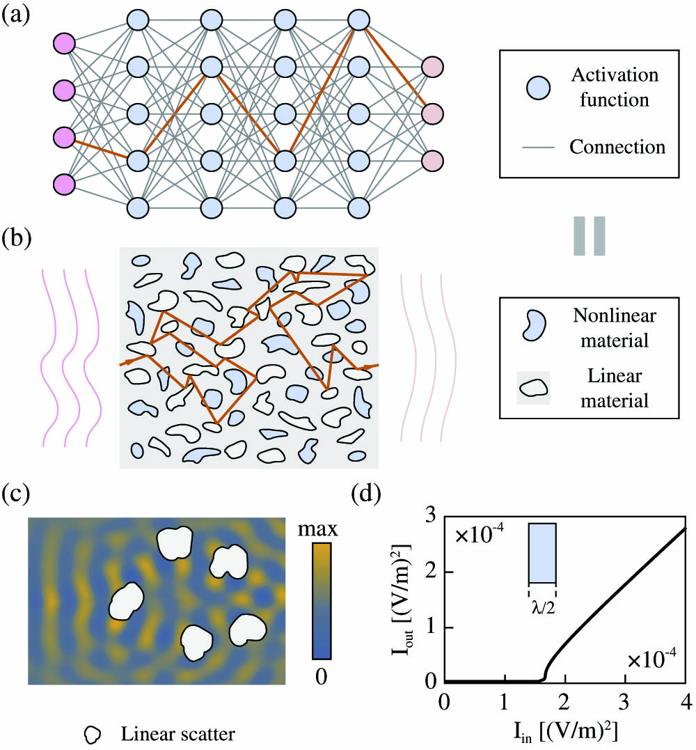
Figure 1.(a) Conventional ANN architecture where the information propagates only in the forward direction (depicted by the green line that goes through the nodes from input to output); (b) proposed NNM. Passive neural computing is performed by light passing through the nanostructured medium with both linear and nonlinear scatterers. (c) Full-wave simulation of light scattered by nanostructures, which spatially redistribute the optical energy in different directions. (d) The behavior of the implementation of such a nonlinear material in one dimension. The output intensity of light with wavelength , passing through the designed nonlinear material with a thickness of . It is a nonlinear function of the incident wave intensity. This material is used as nonlinear activation, as indicated by light blue color.
2. IMPLEMENTATION
Figure 2 shows an NNM in action, where a two-dimensional (2D) medium is trained to recognize gray-scale handwritten digits. The data set contains 5000 different images, representative ones of which are shown in Fig. 2(a). Each time, one image, represented by pixels, is converted to a vector, and then encoded as the spatial intensity of input light incident on the left. Inside the NNM, nanostructures create strong interferences, and light is guided toward one of 10 output locations depending on the digit that the image represents, where the output with the highest share of energy intensity is categorized as the inferred class. Figure 2(b) shows the fields created by two different handwritten 2 digits. Because of different shapes, the field patterns created by these two images are quite different, but both lead to the same hot spot at the output, which correctly identifies the identity information as the number 2. As another example, Fig. 2(c) shows the case of two handwritten 8 digits that result in another hot spot. Here, the field is simulated by solving a nonlinear wave equation using the finite-difference frequency-domain (FDFD [18]) method. The size of the NNM is by , where is the wavelength of light used to carry and process the information. The average recognition accuracy reaches over 79% for a test set made up of 1000 images. The limited reported accuracy is due to the heavy constraints we set during the optimization for fabrication concerns. These constraints keep the medium dense, where it would have been otherwise made up of sparse sections of air and . By relaxing these requirements or using larger medium sizes, accuracy can be further improved.
Sign up for Photonics Research TOC. Get the latest issue of Photonics Research delivered right to you!Sign up now

Figure 2.(a) NNM trained to recognize handwritten digits. The input wave encodes the image as the intensity distribution. On the right side of the NNM, the optical energy concentrates to different locations depending on the image’s classification labels. (b) Two samples of the digit 2 and their optical fields inside the NNM. As can be seen, although the field distributions differ for the images of the same digit, they are classified as the same digit. (c) The same as (b) but for two samples of the digit 8. Also, in both (b) and (c), the boundaries of the trained medium have been shown with black borderlines (see Visualization 1).
Nonlinear nanophotonic media can provide ultra-high density by tapping into sub-wavelength features. In theory, every atom in this medium can be varied to influence the wave propagation. In practice, a change below 10 nm would be considered too challenging for fabrication. Even at this scale, the potential number of weights exceeds 10 billion parameters per square millimeter for a 2D implementation. This is much greater computing density than both free-space [8,19] and on-chip optical neural networks [1,3]. In addition, NNM has a few other attractive features. It has stronger expressive power than layered optical networks. In fact, layered networks are a subset of NNM, as a medium can be shaped into connected waveguides as a layered network. Furthermore, it does not have the issue of diminishing gradients in deep neural networks. Maxwell’s equations, as the governing principle, guarantee that the underlying linear operation is always unitary, which does not have diminishing or exploding gradients [20]. Lastly, NNM does not have to follow any specific geometry, and thus it can be easily shaped and integrated into existing vision or communication devices as the first step of optical preprocessing.
3. TRAINING PROCESS
We now discuss the training of NNM. Although one could envision in situ training of NNM using tunable optical materials [3], here we focus on training in the digital domain and use NNM only for inference. The underlying dynamics of the NNM are governed by the nonlinear Maxwell’s equations, which, in the frequency domain, can be written as where , and and are the permeability and permittivity. is the current source density that represents the spatial profile of the input light and is only nonzero on the left side of the medium. Waveguide modes or plane waves can also be used as the input, which are also implemented as current sources in numerical simulation. For a classification problem, the probability of the th class label is given by , which represents the percentage of energy at the th receiver relative to the total optical energy that reaches all receivers. Here the profile function defines the location of receivers and is only nonzero at the position of the th receiver. The training is performed by optimizing the dielectric constant similar to how weight parameters are trained in traditional neural networks. The cost function is defined by the cross entropy between the output vector and the ground truth : The ground truth is a one-hot vector. Digit 8 is represented as , for instance. The gradient of the cost function with respect to the dielectric constant can be calculated point by point. For example, one could assess the effect of changing at one spatial point; the change is only kept if the loss function decreases. This method has achieved remarkable success in simple photonic devices [13]. However, each gradient calculation requires solving full-wave nonlinear Maxwell’s equations. It is prohibitively costly for NNM, which could easily have millions of gradients. Here, we use the adjoint state method (ASM) to compute all gradients in one step: Here is a Lagrangian multiplier, which is the solution to the adjoint equation [Eq. (4)], in which the electric field is obtained by solving Eq. (1). The adjoint equation here is slightly more involved than what is generally used in inverse design; this is due to the fact that nonlinear behavior is included in our dynamics. A similar derivation for a nonlinear adjoint equation is done in Ref. [21]: The training process, as illustrated in Fig. 3(a), minimizes the summation of the cost functions for all training instances through stochastic gradient descent (SGD). The process starts with one input image as the light source, for which we solve the nonlinear Maxwell’s equations in an iterative process [pink block in Fig. 3(a)]. The initial field is set to be random , which allows us to calculate the dielectric constant . Then FDFD simulation is used to solve Eq. (1), and the resulting electric field is then used to update the dielectric constant. This iteration continues until the field converges. The next step is to compute the gradient based on Eq. (3). Once the structural change is updated, the training of this instance is finished.
Figure 3.(a) Training starts by encoding an image as a vector of current source densities in the FDFD simulation. This step is followed by an iterative process to solve for the electric field in a nonlinear medium. Next, we use the ASM to calculate the gradient, which is then used to update the level-set function and consequently, the medium itself. Here we use mini-batch SGD (explained in the supplementary materials section of Ref. [17]). In training with mini-batches, we sum the cost functions calculated for different images in the same batch and compute the gradients. (b)–(d) show an NNM in training after 1, 33, and 66 training iterations, respectively. (After iteration 66, the medium has already seen each of the training samples at least once, since we are using batches of 100 images.) At each step, the boundary between the host material and the inclusions is shown, along with the field distribution for the same randomly selected digit 8. Also, the accuracy of the medium on the test set can be seen for that particular stage in training.
The above process is repeated again, but for the next different image in the training queue, instead of the same image. This gradient descent process is stochastic, which is quite different from the typical use of ASM in nanophotonics [14,15], where gradient descent is performed repeatedly for very few inputs until the loss function converges. In these traditional optimizations, the device needs to function for only those few specific inputs. If such processes were used here, the medium would do extremely well for particular images but fail to generalize and recognize other images.
The gradient descent process treats the dielectric constant as a continuous variable, but in practice, its value is discrete, depending on the material used at the location. For example, in the case of a medium with host material and linear air inclusions, the dielectric constants can either be 2.16 or 1. Discrete variables remain effective for neural computing [22]. Here, we need to take special care to further constrain the optimization process. This is done by using a level-set function [23], where each of the two materials (host material and the linear inclusion material) is assigned to each of the two levels in the level-set function similar to Refs. [14,15]: The training starts with randomly distributed inclusions, both linear and nonlinear, throughout the host medium. The boundaries between two materials evolve in the training. Specifically, the level-set function is updated by -, where is the gradient calculated by ASM, and indicates the boundary between the two constituent materials. Therefore, at each step, this method essentially decides whether any point on the boundary should be switched from one material to the other. Nonlinear sections perform the activation function, and their location and shape are fixed in this optimization. They could also be optimized, which would be equivalent to optimizing structural hyperparameters in layered neural networks [24–26].
As a specific example, we now discuss the training of the 2D medium shown in Fig. 2. The structural evolution is shown in Figs. 3(b)–3(d) during the training. We start by randomly seeding the domain with dense but small inclusions. As the training progresses, the inclusions move and merge, eventually converging. The recognition accuracy for both the training and test groups improves during this process.
Next, we show another example based on a three-dimensional (3D) medium, whose size is . The inputs can be an image projected on the top surface of the medium. For example, we use a plane wave to illuminate a mask with its opening shaped into a handwritten digit as shown in Fig. 4 (Visualization 2 shows how the energy distribution on the output evolves as a handwritten digit gradually emerges as the input). Fabricating 3D inclusions is generally difficult, but it is much easier to tune the permittivity of materials using direct laser writing [27]. Thus, here we allow the dielectric constant to vary continuously. To save on computational resources, we allow 5% variation. In experimental realization, a smaller variation range can always be compensated for by using larger media. The 3D trained NNM had an accuracy of about 84% for the test set; the confusion matrix is shown in Fig. 4(b). The better performance in comparison with the 2D implementation is due to a higher degree of freedom we allow the dielectric constant to have.
Figure 4.(a) 3D NNM case. Different colors illustrate varying values of permittivity. The input image is projected onto the top surface. Computing is performed while the wave propagates through the 3D medium. The field distribution on the bottom surface is used to recognize the image. Full-wave simulation shows the optical energy is concentrated on the location with the correct class label, in this case 6. (b) The confusion matrix. The rows on the matrix show true labels of the images that have been presented as input, and the columns depict the labels that the medium has classified each input. Therefore, the diagonal elements show the number of correct classifications out of every 10 samples (see Visualization 2).
4. CONCLUSION
Here we show that the wave dynamics in Maxwell’s equations is capable of performing highly sophisticated computing. There is an intricate connection between differential equations that governs many physical phenomena and neural computing (see more discussion in supplementary materials), which could be further explored. From the perspective of optics, the functions of most nanophotonic devices can be described as mode mapping [28]. In traditional nanophotonic devices, mode mapping mostly occurs between eigenmodes. For example, a polarization beam splitter [13] maps each polarization eigenmode to a spatial eigenmode. Here, we introduce a class of nanophotonic media that can perform complex and nonlinear mode mapping equivalent to artificial neural computing. The neural computing media shown here have an appearance of disorder media. It would be also interesting to see how disorder media, which support rich physics such as Anderson localization, could provide a new platform for neural computing. Combined with ultrahigh computing density, NNM could be used in a wide range of information devices as the analog preprocessing unit.
Acknowledgment
Acknowledgment. The authors thank W. Shin for his help on improving the computational speed of the implementation of this method. E. Khoram and Z. Yu thank Shanhui Fan and Momchil Minkov for helpful discussion on nonlinear Maxwell’s equations.
References
[1] Y. Shen, N. C. Harris, S. Skirlo, M. Prabhu, T. Baehr-Jones, M. Hochberg, X. Sun, S. Zhao, H. Larochelle, D. Englund, M. Soljacic. Deep learning with coherent nanophotonic circuits. Nat. Photonics, 11, 441-446(2017).
[2] M. Hermans, M. Burm, T. Van Vaerenbergh, J. Dambre, P. Bienstman. Trainable hardware for dynamical computing using error backpropagation through physical media. Nat. Commun., 6, 6729(2015).
[3] T. W. Hughes, M. Minkov, Y. Shi, S. Fan. Training of photonic neural networks through in situ backpropagation and gradient measurement. Optica, 5, 864-871(2018).
[4] S. R. Skinner, E. C. Behrman, A. A. Cruz-Cabrera, J. E. Steck. Neural network implementation using self-lensing media. Appl. Opt., 34, 4129-4135(1995).
[5] P. R. Prucnal, B. J. Shastri. Neuromorphic Photonics(2017).
[6] H. G. Chen, S. Jayasuriya, J. Yang, J. Stephen, S. Sivaramakrishnan, A. Veeraraghavan, A. Molnar. ASP vision: optically computing the first layer of convolutional neural networks using angle sensitive pixels. Proceedings of the IEEE Conference on Computer Vision and Pattern Recognition, 903-912(2016).
[7] J. Bueno, S. Maktoobi, L. Froehly, I. Fischer, M. Jacquot, L. Larger, D. Brunner. Reinforcement learning in a large-scale photonic recurrent neural network. Optica, 5, 756-760(2018).
[8] X. Lin, Y. Rivenson, N. T. Yardimci, M. Veli, Y. Luo, M. Jarrahi, A. Ozcan. All optical machine learning using diffractive deep neural networks. Science, 361, 1004-1008(2018).
[9] M. Hermans, T. Van Vaerenbergh. “Towards trainable media: Using waves for neural network-style training,”(2015).
[10] H.-G. Park, S.-H. Kim, S.-H. Kwon, Y.-G. Ju, J.-K. Yang, J.-H. Baek, S.-B. Kim, Y.-H. Lee. Electrically driven single-cell photonic crystal laser. Science, 305, 1444-1447(2004).
[11] J. D. Joannopoulos, S. G. Johnson, J. N. Winn, R. D. Meade. Photonic Crystals: Molding the Flow of Light(2011).
[12] W. Cai, V. Shalaev. Optical Metamaterials: Fundamentals and Applications(2009).
[13] B. Shen, P. Wang, R. Polson, R. Menon. An integrated-nanophotonics polarization beamsplitter with 2.4 × 2.4 μm2 footprint. Nat. Photonics, 9, 378-382(2015).
[14] A. Y. Piggott, J. Petykiewicz, L. Su, J. Vučković. Fabrication constrained nanophotonic inverse design. Sci. Rep., 7, 1786(2017).
[15] L. Su, A. Y. Piggott, N. V. Sapra, J. Petykiewicz, J. Vuckovic. Inverse design and demonstration of a compact on-chip narrowband three-channel wavelength demultiplexer. ACS Photon., 5, 301-305(2017).
[16] V. Nair, G. E. Hinton. Rectified linear units improve restricted Boltzmann machines. Proceedings of the 27th International Conference on Machine Learning (ICML-10), 807-814(2010).
[17] E. Khoram, A. Chen, D. Liu, Q. Wang, Z. Yu, L. Ying. Nanophotonic media for artificial neural inference(2018).
[18] W. Shin. MaxwellFDFD.
[19] H. J. Caulfield, J. Kinser, S. K. Rogers. Optical neural networks. Proc. IEEE, 77, 1573-1583(1989).
[20] L. Jing, Y. Shen, T. Dubcek, J. Peurifoy, S. Skirlo, Y. LeCun, M. Tegmark, M. Soljačić. Tunable efficient unitary neural networks (EUNN) and their application to RNNs. Proceedings of the 34th International Conference on Machine Learning (PMLR), 1733-1741(2017).
[21] T. W. Hughes, M. Minkov, I. A. Williamson, S. Fan. Adjoint method and inverse design for nonlinear nanophotonic devices. ACS Photon., 5, 4781-4787(2018).
[22] M. Courbariaux, I. Hubara, D. Soudry, R. El-Yaniv, Y. Bengio. Binarized neural networks: training deep neural networks with weights and activations constrained to +1 or -1(2016).
[23] C. Li, C. Xu, C. Gui, M. D. Fox. Distance regularized level-set evolution and its application to image segmentation. IEEE Trans. Image Process., 19, 1371-1378(2010).
[24] J. Bergstra, Y. Bengio. Random search for hyper-parameter optimization. J. Mach. Learn. Res., 13, 281-305(2012).
[25] J. Snoek, H. Larochelle, R. P. Adams. Practical Bayesian optimization of machine learning algorithms. Advances in Neural Information Processing Systems, 2951-2959(2012).
[26] S. Saxena, J. Verbeek. Convolutional neural fabrics. Advances in Neural Information Processing Systems, 4053-4061(2016).
[27] G. D. Marshall, A. Politi, J. C. Matthews, P. Dekker, M. Ams, M. J. Withford, J. L. O’Brien. Laser written waveguide photonic quantum circuits. Opt. Express, 17, 12546-12554(2009).
[28] D. A. Miller. All linear optical devices are mode converters. Opt. Express, 20, 23985-23993(2012).


